

SGS Thomson Microelectronics 74LVC14ATTR, 74LVC14AMTR, 74LVC14AM Datasheet
1/9December 2002
■ 5V TOLERANT INPUTS
■ HIGH SPEED:t
PD
= 5. 0ns (MAX.) at VCC=3V
■ POWER DOWN PROTECTION ON INPUTS
AND OUTPUTS
■ SYMMETRICAL OUTPUT IMPEDANCE:
|I
OH
|=IOL= 24mA (MIN) at VCC=3V
■ PCI BUS LEVELS GUARANTEEDAT 24 mA
■ BALANCED PROPAGATION DELAYS:
t
PLH
≅ t
PHL
■ OPERATING VOLTAGE RANGE:
V
CC
(OPR) = 1.65V to 3.6V (1.2V Data
Retention)
■ PIN AND FUNCTION COMPATIBLE WITH
74 SERIES 00
■ LATCH-UP PERFORMANCE EXCEEDS
500mA (JESD 17)
■ ESD PERFORMANCE:
HBM > 2000V (MIL STD 883 method 3015);
MM > 200V
DESCRIPTION
The 74LVC14A is a low voltage CMOS HEX
SCHMITT INVERTER fabricated with sub-micron
silicon gate and double -layer metal wiring C
2
MOS
technology. I t is ideal for 1.65 to 3.6 V
CC
operations and low power and low noise
applications.
It can be interfaced to 5V signal environm ent f or
inputs in mixed 3.3/5V system.
It has more speed performance a t 3.3V than 5V
AC/ACT family, combined with a lower power
consumption.
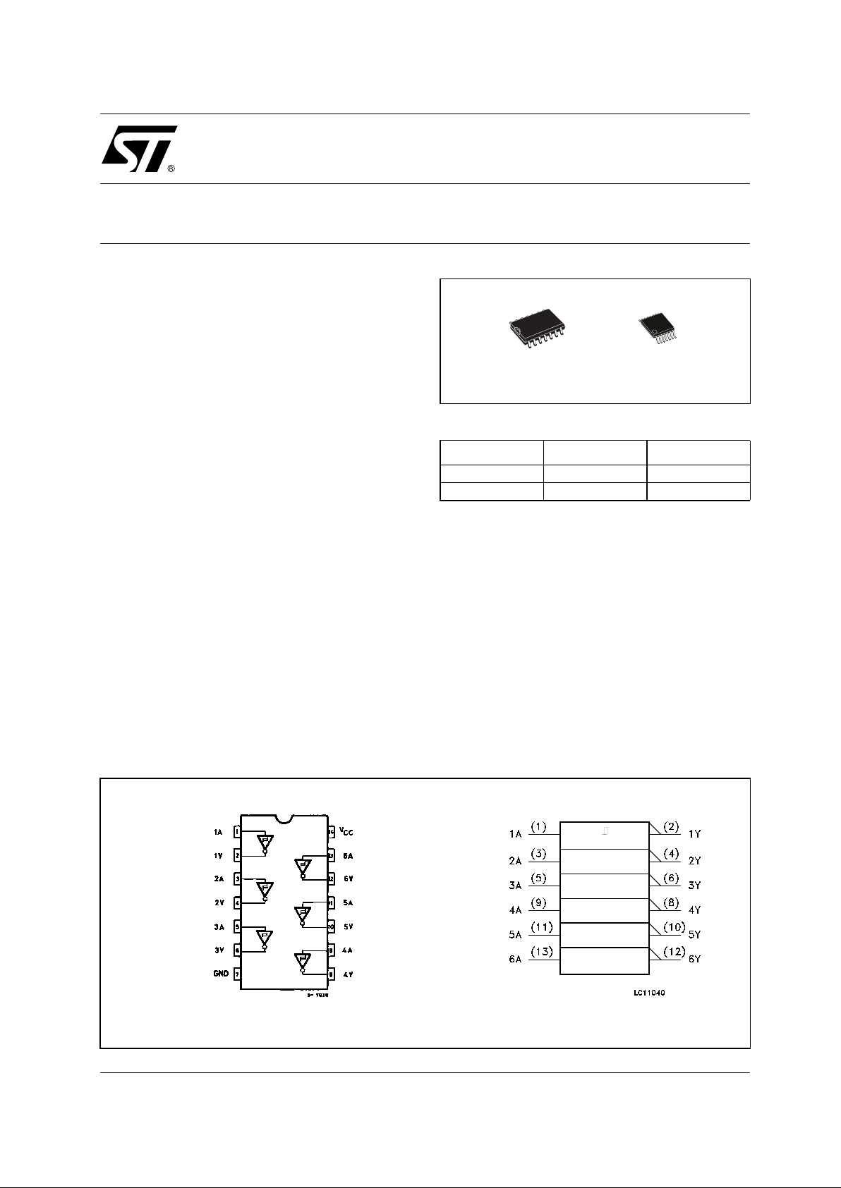
Pin configuration and function are the same as
those of the 74LVC04A but the 74LVC14A has
hysteresis between the positive and negative
input threshold typically of 700mV.
All inputs and outputs are e quipped with
protection circuits aga inst static discharge, giving
them 2KV ESD immunity and transient excess
voltage.
74LVC14A
LOW VOLTAGE CMOS HEX INVERTER
HIGH PERFORMANCE
PIN CONNECTION AND IEC LOGIC SYMBOLS
ORDER CODES
PACKAGE TUBE T & R
SOP 74LVC14AM 74LVC14AMTR
TSSOP 74LVC14ATTR
TSSOPSOP
74LVC14A
2/9
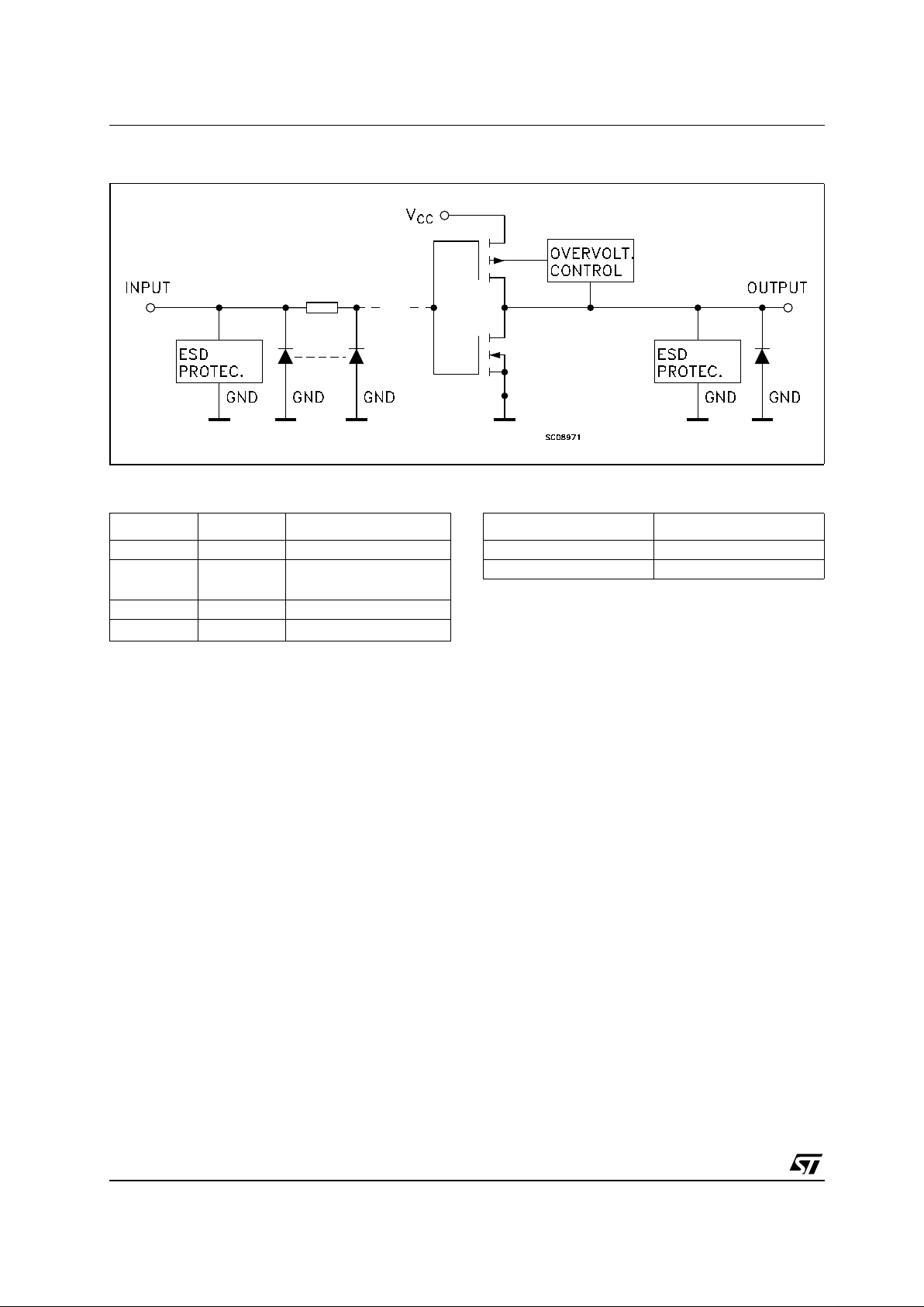
INPUT AND O UTPUT EQUIVALENT CIRCUIT
PIN DESCRIPTION TRUTH TABLE
PIN No SYMBOL NAME AND FUNCTION
1,3,5,9,11,13 1A to 6A Data Inputs
2, 4, 6, 8,
10, 12
1Y to 6Y Data Outputs
7 GND Ground (0V)
14
V
CC
Positive Supply Voltage
AY
LH
HL
74LVC14A
3/9
ABSOLUTE MAXIMUM RATINGS
Absolute Maximum Ratings are those values beyond which damage to the device may occur. Functional operation under these conditions is
not implied
1) I
O
absolute maximum rating must be observed
2) V
O
<GND
RECOMMENDED OPERATING CONDITIONS
1) Truth Table guaranteed: 1.2V to 3.6V
Symbol Parameter Value Unit
V
CC
Supply Voltage
-0.5 to +7.0 V
V
I
DC Input Voltage
-0.5 to +7.0 V
V
O
DC Output Voltage (VCC= 0V)
-0.5 to +7.0 V
V
O
DC Output Voltage (High or Low State) (note 1) -0.5 to VCC+ 0.5
V
I
IK
DC Input Diode Current
-50 mA
I
OK
DC Output Diode Current (note 2)
-50 mA
I
O
DC Output Current
± 50 mA
I
CC
or I
GND
DC VCCor Ground Current per Supply Pin
± 100 mA
T
stg
Storage Temperature
-65 to +150 °C
T
L
Lead Temperature (10 sec)
300 °C
Symbol Parameter Value Unit
V
CC
Supply Voltage (note 1)
1.65 to 3.6 V
V
I
Input Voltage
0 to 5.5 V
V
O
Output Voltage (VCC= 0V)
0 to 5.5 V
V
O
Output Voltage (High or Low State) 0 to V
CC
V
I
OH,IOL
High or Low Level Output Current (VCC= 3.0 to 3.6V)
± 24 mA
I
OH,IOL
High or Low Level Output Current (VCC= 2.7 to 3.0V)
± 12 mA
I
OH,IOL
High or Low Level Output Current (VCC= 2.3 to 2.7V)
± 8mA
I
OH,IOL
High or Low Level Output Current (VCC= 1.65 to 2.3V)
± 4mA
T
op
Operating Temperature
-55 to 125 °C
 Loading...