

1/8February 2002
■ 5V TOLERANT INPUTS
■ HIGH SPEED: t
PD
= 4.5ns (MAX.) at VCC = 3V
■ POWER DOWN PROTECTION ON INPU T S
AND OUTPUTS
■ SYMMETRICAL OUTPUT IMPEDANCE:
|I
OH
| = IOL = 24mA (MIN) at VCC = 3V
■ PCI BUS LEVELS GUARANT EED AT 2 4 mA
■ BALANCED PROPAGATION DELAYS:
t
PLH
≅ t
PHL
■ OPERATING VOLTAGE RANGE:
V
CC
(OPR) = 1.65V to 3.6V (1.2V Data
Retention)
■ PIN AND FUNCTION COMPATIBLE WITH
74 SERIES 00
■ LATCH-UP PERFORMANCE EXCEEDS
500mA (JESD 17)
■ ESD PERFORMANCE:
HBM > 2000V (MIL STD 883 method 3015);
MM > 200V
DESCRIPTION
The 74LVC04A is a low voltage CMOS HEX
INVERTER fabricated with sub-micron silicon
gate and double-layer metal wiring C
2
MOS
technology. It is ideal for 1.65 to 3.6 V
CC
operations and low power and low noise
applications.
It can be interfaced to 5V signal environment for
inputs in mixed 3.3/5V system.
It has more speed performance at 3.3V than 5V
AC/ACT family, combined with a lower power
consumption.
All inputs and outputs are equipped with
protection circuits against stat ic discharge, giving
them 2KV ESD immunity and transient excess
voltage.
74LVC04A
LOW VOLTAGE CMOS HEX INVERTER
HIGH PERFORMANCE
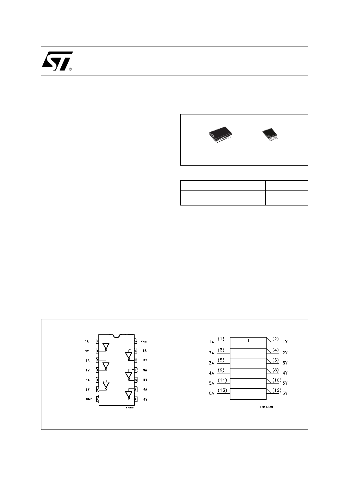
PIN CONNECTION AND IEC LOGIC SYMBOLS
ORDER CODES
PACKAGE TUBE T & R
SOP 74LVC04AM 74LVC04AMTR
TSSOP 74LVC04ATTR
TSSOPSOP
74LVC04A
2/8
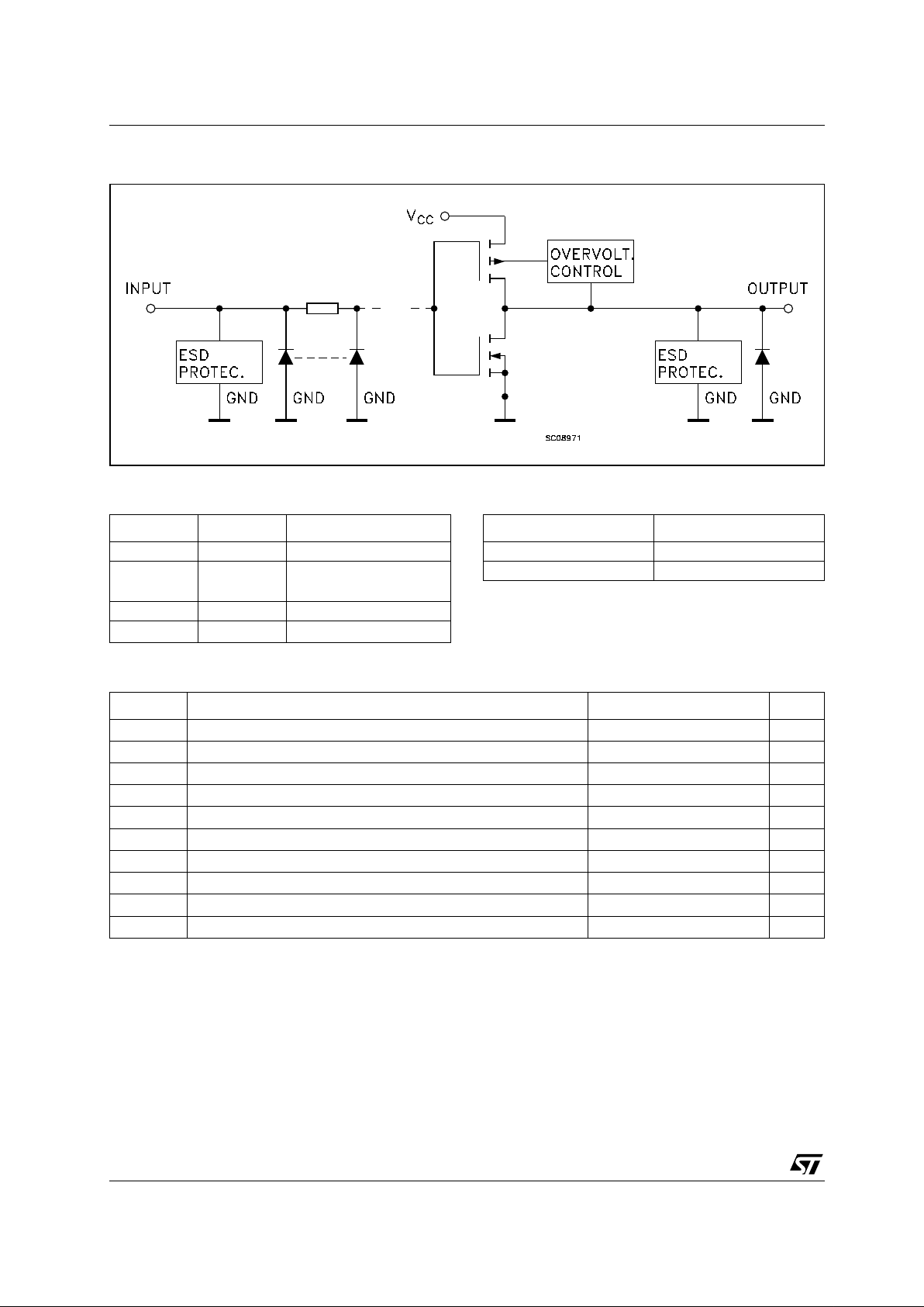
INPUT AND OUTPUT EQUIVALENT CIRCUIT
PIN DESCRIPTION TRUTH TABLE
ABSOLUTE MAXIMUM RATINGS
Absolute Maximum Ratings are those values beyond which damage to the device may occur. Functional operation under these conditions is
not implied
1) I
O
absolute ma xim um rating must be obse rved
2) V
O
< GND
PIN No SYMBOL NAME AND FUNCTION
1,3,5,9,11,13 1A to 6A Data Inputs
2, 4, 6, 8,
10, 12
1Y to 6Y Data Outputs
7 GND Ground (0V)
14
V
CC
Positive Supply Voltage
AY
LH
HL
Symbol Parameter Value Unit
V
CC
Supply Voltage
-0.5 to +7.0 V
V
I
DC Input Voltage
-0.5 to +7.0 V
V
O
DC Output Voltage (VCC = 0V)
-0.5 to +7.0 V
V
O
DC Output Voltage (High or Low State) (note 1) -0.5 to VCC + 0.5
V
I
IK
DC Input Diode Current
- 50 mA
I
OK
DC Output Diode Current (note 2)
- 50 mA
I
O
DC Output Current
± 50 mA
I
CC
or I
GND
DC VCC or Ground Current per Supply Pin
± 100 mA
T
stg
Storage Temperature
-65 to +150 °C
T
L
Lead Temperature (10 sec)
300 °C
74LVC04A
3/8
RECOMMENDED OPERATING CONDITIONS
1) Truth T abl e guarante ed: 1.2V to 3.6 V
2) V
IN
from 0.8V to 2V at VCC = 3.0V
DC SPECIFICATIONS
Symbol Parameter Value Unit
V
CC
Supply Voltage (note 1)
1.65 to 3.6 V
V
I
Input Voltage
0 to 5.5 V
V
O
Output Voltage (VCC = 0V)
0 to 5.5 V
V
O
Output Voltage (High or Low State) 0 to V
CC
V
I
OH
, I
OL
High or Low Level Output Current (VCC = 3.0 to 3.6V)
± 24 mA
I
OH
, I
OL
High or Low Level Output Current (VCC = 2.7 to 3.0V)
± 12 mA
I
OH
, I
OL
High or Low Level Output Current (VCC = 2.3 to 2.7V)
± 8mA
I
OH
, I
OL
High or Low Level Output Current (VCC = 1.65 to 2.3V)
± 4mA
T
op
Operating Temperature
-55 to 125 °C
dt/dv Input Rise and Fall Time (note 2) 0 to 10 ns/V
Symbol Parameter
Test Condition Value
Unit
V
CC
(V)
-40 to 85 °C -55 to 125 °C
Min. Max. Min. Max.
V
IH
High Level Input
Voltage
1.65 to 1.95
0.65V
CC
0.65V
CC
V
2.3 to 2.7 1.7 1.7
2.7 to 3.6 2 2
V
IL
Low Level Input
Voltage
1.65 to 1.95
0.35V
CC
0.35V
CC
V
2.3 to 2.7 0.7 0.7
2.7 to 3.6 0.8 0.8
V
OH
High Level Output
Voltage
1.65 to 3.6
IO=-100 µAVCC-0.2 VCC-0.2
V
1.65
I
O
=-4 mA
1.2 1.2
2.3
I
O
=-8 mA
1.7 1.7
2.7
I
O
=-12 mA
2.2 2.2
3.0
I
O
=-18 mA
2.4 2.4
3.0
I
O
=-24 mA
2.2 2.2
V
OL
Low Level Output
Voltage
1.65 to 3.6
IO=100 µA
0.2 0.2
V
1.65
I
O
=4 mA
0.45 0.45
2.3
I
O
=8 mA
0.7 0.7
2.7
I
O
=12 mA
0.4 0.4
3.0
I
O
=24 mA
0.55 0.55
I
I
Input Leakage
Current
3.6
V
I
= 0 to 5.5V
± 5 ± 5 µA
I
off
Power Off Leakage
Current
0
V
I
or VO = 5.5V
100 100 µA
I
CC
Quiescent Supply
Current
3.6
VI = VCC or GND
10 10
µA
V
I
or VO = 3.6 to
5.5V
± 10 ± 10
∆I
CC
ICC incr. per Input
2.7 to 3.6
VIH = VCC-0.6V
500 500 µA

74LVC04A
4/8
DYNAMIC SWITCHING CHARACTERISTICS
1) Number of output defined as "n". Measured with "n-1" outputs switc hi ng from HIGH to LOW or LOW to H IGH. The remai ning outp ut is
measur ed i n the LOW sta te.
AC ELECTRICAL CHARACTERISTICS
1) Skew is defined as the absolute value of the difference between the actual propagation delay for any two outputs of the same device switching in the same direction, either HIGH or LOW ( t
OSLH
= | t
PLHm
- t
PLHn
|, t
OSHL
= | t
PHLm
- t
PHLn
|
2) Param eter guaranteed by design
CAPACITIVE CHARACTERISTICS
1) CPD is defined as the value of the IC’s internal equivalent capacitance which is calculated from the operating current consumption without
load. (Refer to Test Circuit). Average operating current can be obtained by the following equation. I
CC(opr)
= CPD x VCC x fIN + ICC/n (per c ircuit )
Symbol Parameter
Test Condition Value
Unit
V
CC
(V)
T
A
= 25 °C
Min. Typ. Max.
V
OLP
Dynamic Low Level Quiet
Output (note 1)
3.3
C
L
= 50pF
V
IL
= 0V, VIH = 3.3V
0.8
V
V
OLV
-0.8
Symbol Parameter
Test Condition Value
Unit
V
CC
(V)
C
L
(pF)
R
L
(Ω)
t
s
= t
r
(ns)
-40 to 85 °C -55 to 125 °C
Min. Max. Min. Max.
t
PLH tPHL
Propagation Delay
Time
1.65 to 1.95 30 1000 2.0 9.5 12.5
ns
2.3 to 2.7 30 500 2.0 7.0 10
2.7 50 500 2.5 5.5 6.6
3.0 to 3.6 50 500 2.5 1 4.5 1 5.4
t
OSLH
t
OSHL
Output To Output
Skew Time (note1,
2)
2.7 to 3.6 1 1 ns
Symbol Parameter
Test Condition Value
Unit
V
CC
(V)
T
A
= 25 °C
Min. Typ. Max.
C
IN
Input Capacitance
4pF
C
PD
Power Dissipation Capacitance
(note 1)
1.8 fIN = 10MHz 37
pF2.5 37
3.3 41

74LVC04A
5/8
TEST CIRCUIT
RT = Z
OUT
of pulse generator (typically 50Ω)
TEST CIRCUIT AND WAVEFORM SYMBOL VALUE
WAVEFORM: PROPAGATION DELAY (f=1 MHz; 5 0 % duty cycle)
Symbol
V
CC
1.65 to 1.95V 2.3 to 2.7V 2.7V 3.0 to 3.6V
C
L
30pF 30pF 50pF 50pF
R
L
1000Ω 500Ω 500Ω 500Ω
V
IH
V
CC
V
CC
2.7V 2.7V
V
M
VCC/2 VCC/2 1.5V 1.5V
V
OH
V
CC
V
CC
3.0V 3.0V
t
r
= t
r
<2.0ns <2.0ns <2.5ns <2.5ns

74LVC04A
6/8
DIM.
mm. inch
MIN. TYP MAX. MIN. TYP. MAX.
A 1.75 0.068
a1 0.1 0.2 0.003 0.007
a2 1.65 0.064
b 0.35 0.46 0.013 0.018
b1 0.19 0.25 0.007 0.010
C 0.5 0.019
c1 45° (typ.)
D 8.55 8.75 0.336 0.344
E 5.8 6.2 0.228 0.244
e 1.27 0.050
e3 7.62 0.300
F 3.8 4.0 0.149 0.157
G 4.6 5.3 0.181 0.208
L 0.5 1.27 0.019 0.050
M 0.68 0.026
S8° (max.)
SO-14 MECHANICAL DATA
PO13G

74LVC04A
7/8
DIM.
mm. inch
MIN. TYP MAX. MIN. TYP. MAX.
A 1.2 0.047
A1 0.05 0.15 0.002 0.004 0.006
A2 0.8 1 1.05 0.031 0.039 0.041
b 0.19 0.30 0.007 0.012
c 0.09 0.20 0.004 0.0089
D 4.9 5 5.1 0.193 0.197 0.201
E 6.2 6.4 6.6 0.244 0.252 0.260
E1 4.3 4.4 4.48 0.169 0.173 0.176
e 0.65 BSC 0.0256 BSC
K0° 8°0° 8°
L 0.45 0.60 0.75 0.018 0.024 0.030
TSSOP14 MECHANICAL DATA
c
E
b
A2
A
E1
D
1
PIN 1 IDENTIFICATION
A1
L
K
e
0080337D

74LVC04A
8/8
Information furnished is believed to be accurate and reliable. However, STMicroelectronics assumes no responsibilit y for t he
consequences of use of such informatio n nor for any infringement of paten ts or o ther rig hts of t hird part ies which ma y result from
its use. No license is granted by implication or otherwise under any patent or patent rights of STMicroelectronics. Specifications
mentioned in this publication are subject to change without notice. This publication supersedes and replaces all information
previousl y suppl ied. STM icroel ectronics produc ts are not auth orized for use as c ritica l compone nts in l ife s upport dev ices or
systems without express written approval of STMicroelectronics.
© The ST logo is a registered trademark of STMicroelectronics
© 2002 STMicroelectronics - Printed in Italy - All Rights Reserved
STMicroelectronics GROUP OF COMPANIES
Australia - Brazil - Canada - China - Finland - France - Germany - Hong Kong - India - Israel - Italy - Japan - Malaysia - Malta - Morocco
Singapore - Spain - Sweden - Switzerland - United Kingdom - United States.
© http://www.st.com
 Loading...