

SGS Thomson Microelectronics 74LCX652M, 74LCX652TTR, 74LCX652MTR Datasheet
1/13September 2001
■ 5V TOLERANT INPUTS AND OUTPUTS
■ HIGH SPEED :
t
PD
= 7.0 ns (MAX.) at VCC = 3V
■ POWER DOWN PROTECTION ON INPUT S
AND OUTPUTS
■ SYMMETRICAL OUTPUT IMPEDANCE:
|I
OH
| = IOL = 24mA (MIN) at VCC = 3V
■ PCI BUS LEVELS GUARANT EED AT 2 4 mA
■ BALANCED PROPAGATION DELAYS:
t
PLH
≅ t
PHL
■ OPERATING VOLTAGE RANGE:
V
CC
(OPR) = 2.0V to 3.6V (1.5V Data
Retention)
■ PIN AND FUNCTION COMPATIBLE WITH
74 SERIES 652
■ LATCH-UP PERFORMANCE EXCEEDS
500mA (JESD 17)
■ ESD PERFORMANCE:
HBM > 2000V (MIL STD 883 method 3015);
MM > 200V
DESCRIPTION
The 74LCX652 is a low voltage CMOS OCTAL
BUS TRANSCEIVER AND REGISTER
(3-ST AT E ) fab r ic ated with sub-mic r on silic o n g at e
and double-layer metal wiring C
2
MOS technology.
It is ideal for low power and high speed 3.3V
applications; it can be interfaced to 5V signal
environment for both inputs and outputs.
This device consists of bus transceiver circuits
with 3 state, D-type flip-flops, and control circuitry
arranged for multiplexed transmission of data
directly from the input bus or from the internal
storage registers. Enab le (GAB) and (GBA
) pins
are provided to control the transceiver functions.
Select AB and Select BA control pins are provided
to select whether real-time or stored data is
transferred. A low input level selects real-time,
and a high selects stored data.
Data on the A or B bus, or both, can be stored i n
the internal D flip-flop by l ow to high transitions at
the appropriate clock pins (CAB or CBA)
regardless of the select or enable control pins.
When select AB and select BA are in the real-time
transfer mode, it is also possible to store data
74LCX652
LOW VOLT. CMOS OCTAL BUS TRANSCEIVER/REGISTER
WITH 5 VOLT TOLERANT INPUTS AND OUTPUTS(3-STATE)
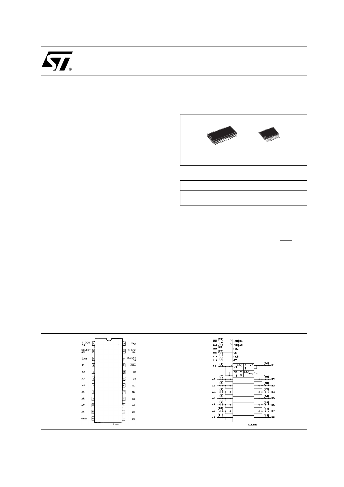
PIN CONNECTION AND IEC LOGIC SYMBOLS
ORDER CODES
PACKAGE TUBE T & R
SOP 74LCX652M1R 74LCX652RM13TR
TSSOP 74LCX652TTR
TSSOPSOP
M74LCX652
2/13
without using the internal D-type flip-flops by
simultaneously enabling GAB or GBA
. In this
configuration each output reinforces its input.
It has same speed performance at 3. 3V than 5V
AC/ACT family, combined with a lower power
consumption.
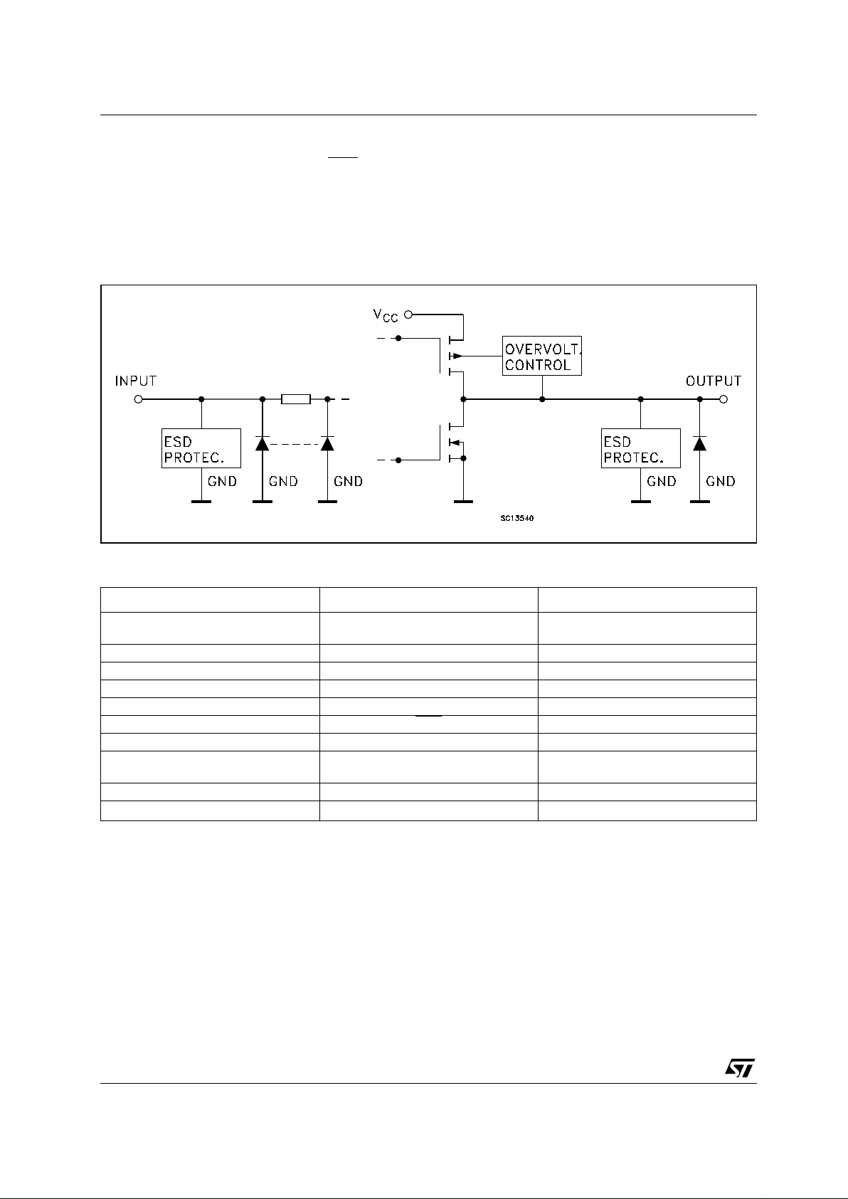
All inputs and outputs are equipped with
protection circuits against stat ic discharge, giving
them 2KV ESD immunity and transient excess
voltage.
INPUT AND OUTPUT EQUIVALENT CIRCUIT
PIN DESCRIPTION
PIN No SYMBOL NAME AND FUNCTION
1 CLOCK AB (CAB) A to B Clock Input (LOW to HIGH,
Edge-Triggered)
2 SELECT AB (SAB) Select A to B Source Input
3 GAB Direction Control Input
4, 5, 6, 7, 8, 9, 10, 11 A1 to A8 A Data Inputs/Outputs
20, 19, 18, 17, 16, 15, 14, 13 B1 to B8 B Data Inputs/Outputs
21 GBA
Output Enable Input (Active LOW)
22 SELECT BA (SBA) Select B to A Source Input
23 CLOCK BA (CBA) B to A Clock Input (LOW to HIGH,
Edge Triggered)
12 GND Ground (0V)
24 V
CC
Positive Supply Voltage
M74LCX652
3/13
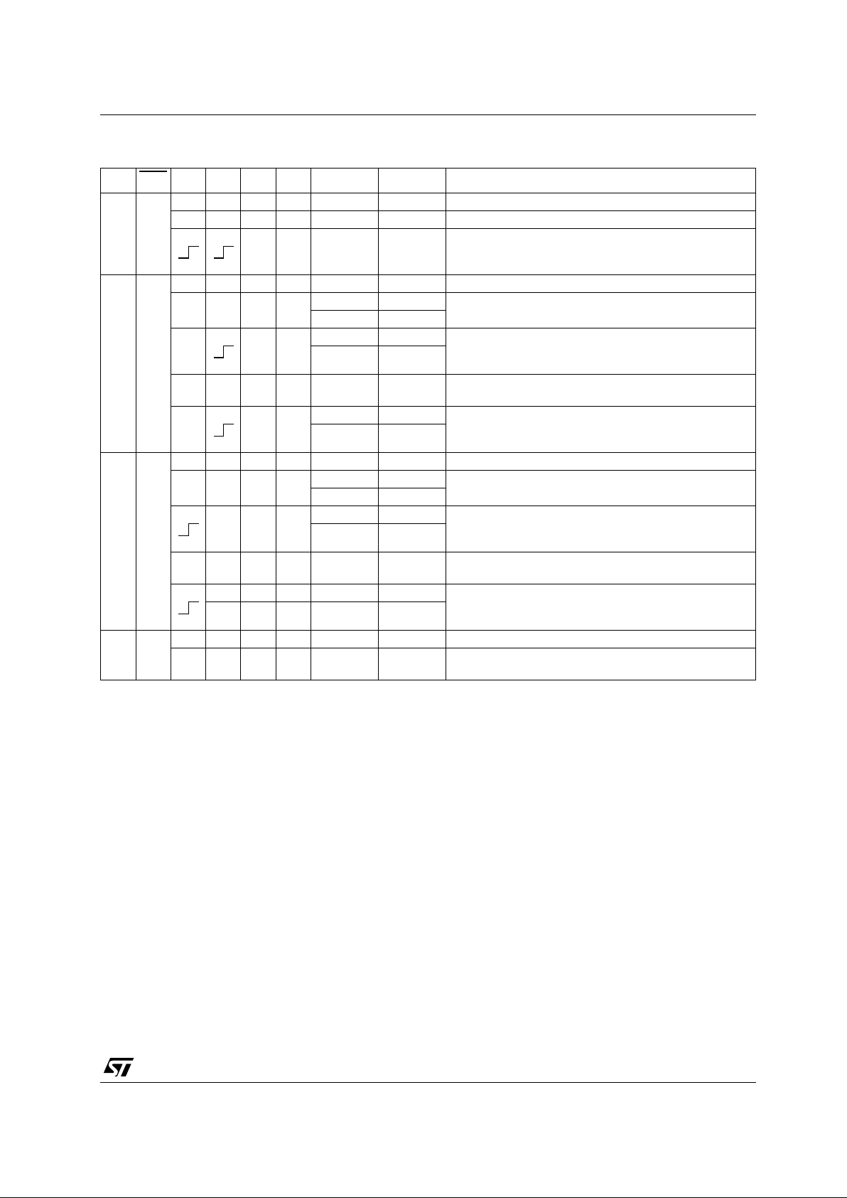
TRUTH TABLE
X : Don’t Care
Z : High Impedance
Qn : The data stored to the internal flip-flops by mo st recent low to hi gh transition of t he clock input s
* : The data at the A and B bus will be stored to the internal flip-flops on every low to high transition of the clock inputs.
GAB GBA C AB CBA SAB SBA A B FUNCTION
LH
INPUTS INPUTS Both the A bus and the B bus are inputs
X X X X Z Z The Output functions of the A and B bus are disabled
X X INPUTS INPUTS
Both the A and B bus are used for inputs to the internal
flip-flops. Data at the bus will be stored on low to high
transition of the clock inputs.
LL
OUTPUTS INPUTS The A bus are outputs and the B bus are inputs
X* X X L
LL
The data at the B bus are displayed at the A bus
HH
X* X L
L L The data at the B bus are displayed at the A bus. The
data of the B bus are stored to internal flip-flop on low
to high transition of the clock pulse
HH
X*XXH Qn X
The data stored to the internal flip-flop are displayed at
the A bus.
X* X H
L L The data at the B bus are stored to the internal flip-flop
on low to high transition of the clock pulse. The states
of the internal flip-flops output directly to the A bus.
HH
HH
INPUTS OUTPUTS The A bus are inputs and the B bus are outputs.
XX*L X
LL
The data at the A bus are displayed at the B bus
HH
X* L X
L L The data at the A bus are displayed at the B bus. The
data of the A bus are stored to the internal flip-flop on
low to high transition of the clock pulse.
HH
XX*HX X Qn
The data stored to the internal flip-flops are displayed
at the B bus
X* H X L L The data at the A bus are stored to the internal flip-flop
on low to high transition of the clock pulse. The states
of the internal flip-flops output directly to the B bus.
X* H X H H
HL
OUTPUTS OUTPUTS Both the A bus and the B bus are outputs
X X H H Qn Qn
The data stored to the internal flip-flops are displayed
at the A and B bus respectively.
M74LCX652
4/13
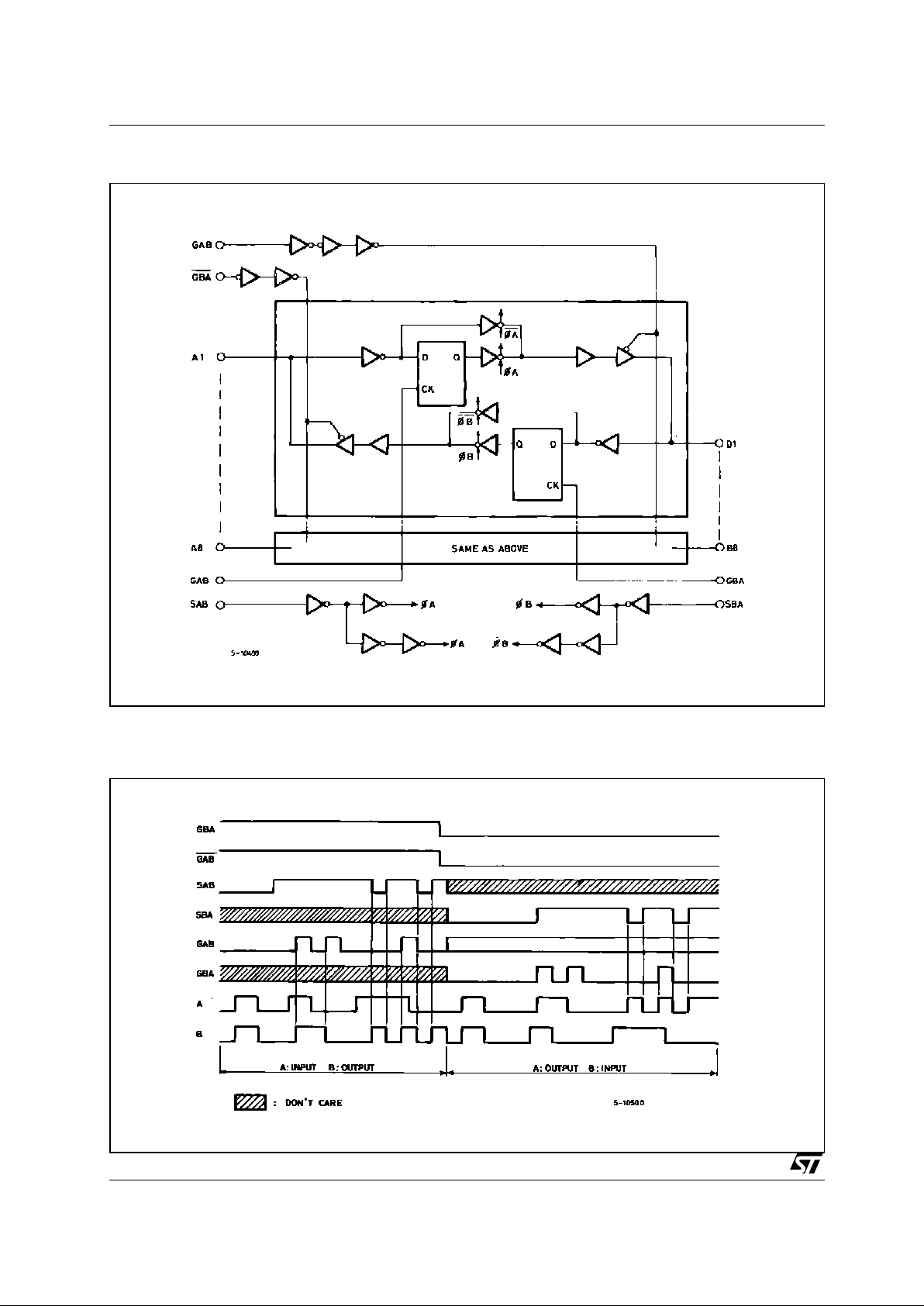
LOGIC DIAGRAM
This log i c diagram has not be used to esti m ate propaga tion delays
TIMING CHART
 Loading...