

1/13September 2001
■ 5V TOLERANT INPUTS AND OUTPUTS
■ HIGH SPEED :
t
PD
= 7.0 ns (MAX.) at VCC = 3V
■ POWER DOWN PROTECTION ON INPUT S
AND OUTPUTS
■ SYMMETRICAL OUTPUT IMPEDANCE:
|I
OH
| = IOL = 24mA (MIN) at VCC = 3V
■ PCI BUS LEVELS GUARANT EED AT 2 4 mA
■ BALANCED PROPAGATION DELAYS:
t
PLH
≅ t
PHL
■ OPERATING VOLTAGE RANGE:
V
CC
(OPR) = 2.0V to 3.6V (1.5V Data
Retention)
■ PIN AND FUNCTION COMPATIBLE WITH
74 SERIES 646
■ LATCH-UP PERFORMANCE EXCEEDS
500mA (JESD 17)
■ ESD PERFORMANCE:
HBM > 2000V (MIL STD 883 method 3015);
MM > 200V
DESCRIPTION
The 74LCX646 is a low voltage CMOS OCTAL
BUS TRANSCEIVER AND REGISTER
(3-ST AT E ) fab r ic ated with sub-mic r on silic o n g at e
and double-layer metal wiring C
2
MOS technology.
It is ideal for low power and high speed 3.3V
applications; it can be interfaced to 5V signal
environment for both inputs and outputs.
This device consists of bus transceiver circuits
with 3 state, D-type flip-flops, and control circuitry
arranged for multiplexed transmission of data
directly from the input bus or from the internal
registers. Data on the A or B bus will be clocked
into register on the low to high transition of the
appropriate clock pin (Clock AB or Clock BA).
Enable (G
) and direction (DIR) pins are provided
to control the transceiver functions. In the
transceiver mode, data present at the
high-impedance port may be stored in either
register or in both. The select controls (Select AB
select BA) can multiplex stored and real time
(transparent mode) data. The direction control
determines which bus will receive data when
enable G
is active (low). In the isolation mode
74LCX646
LOW VOLT. CMOS OCTAL BUS TRANSCEIVER/REGISTER
WITH 5 VOLT TOLERANT INPUTS AND OUTPUTS(3-STATE)
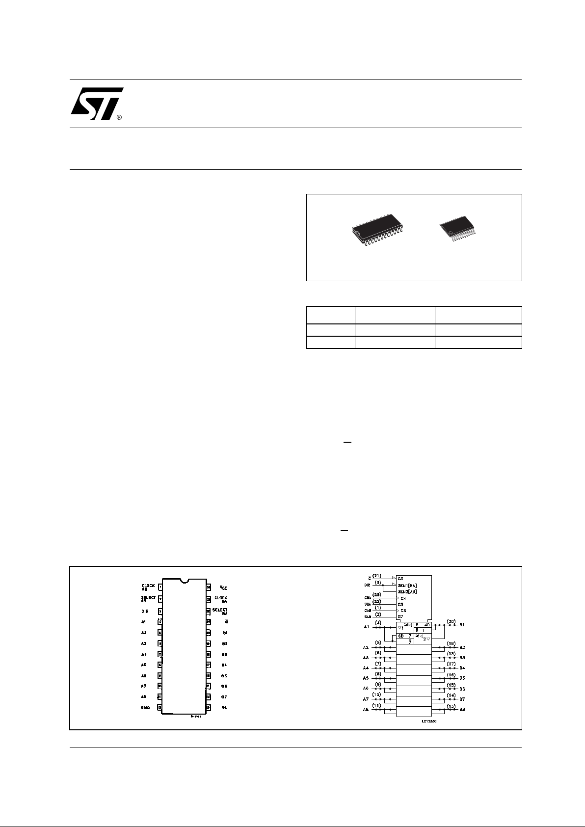
PIN CONNECTION AND IEC LOGIC SYMBOLS
ORDER CODES
PACKAGE TUBE T & R
SOP 74LCX646M1R 74LCX646RM13TR
TSSOP 74LCX646TTR
TSSOPSOP

M74LCX646
2/13
(enable G high), "A" data may be stored in one
register and/or "B" data may be stored in the other
register. When a n output func tion is disabl ed, the
input function is still enabled a nd m ay be used to
store and transmit data. Only one of the two
buses, A or B, may be driven at a time. It has
same speed performance at 3.3V than 5V
AC/ACT family, combined with a lower power
consumption.
All inputs and outputs are equipped with
protection circuits against stat ic discharge, giving
them 2KV ESD immunity and transient excess
voltage.
INPUT AND OUTPUT EQUIVALENT CIRCUIT
PIN DESCRIPTION
PIN No SYMBOL NAME AND FUNCTION
1 CLOCK AB (CAB) A to B Clock Input (LOW to HIGH,
Edge-Triggered)
2 SELECT AB (SAB) Select A to B Source Input
3 DIR Direction Control Input
4, 5, 6, 7, 8, 9, 10, 11 A1 to A8 A Data Inputs/Outputs
20, 19, 18, 17, 16, 15, 14, 13 B1 to B8 B Data Inputs/Outputs
21 G
Output Enable Input (Active LOW)
22 SELECT BA (SBA) Select B to A Source Input
23 CLOCK BA (CBA) B to A Clock Input (LOW to HIGH,
Edge Triggered)
12 GND Ground (0V)
24 V
CC
Positive Supply Voltage
M74LCX646
3/13
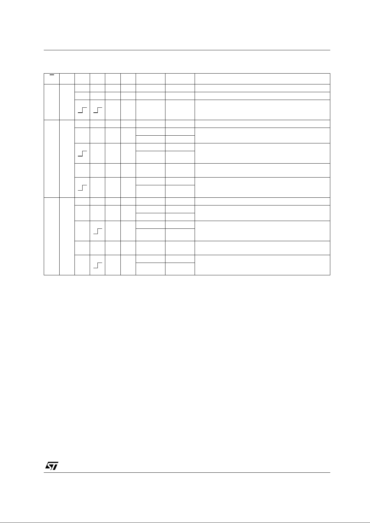
TRUTH TABLE
X : Don’t Care
Z : High Impedance
Qn : The data stored to the internal flip-flops by mo st recent low to hi gh transition of t he clock input s
* : The data at the A and B bus will be stored to the internal flip-flops on every low to high transition of the clock inputs.
G DIR CAB CBA SAB SB A A B FUNCTION
HX
INPUTS INPUTS Both the A bus and the B bus are inputs
X X X X Z Z The Output functions of the A and B bus are disabled
X X INPUTS INPUTS
Both the A and B bus are used as inputs to the internal
flip-flops. Data at the bus will be stored on low to high
transition of the clock inputs.
LH
INPUTS OUTPUTS The A bus are inputs and the B bus are outputs
XX*L X
LL
The data at the A bus are displayed at the B bus
HH
X* L X
L L The data at the A bus are displayed at the B bus. The
data of the A bus are stored to internal flip-flop on low
to high transition of the clock pulse
HH
XX*HX X Qn
The data stored to the internal flip-flop are displayed at
the B bus.
X* H X
L L The data at the A bus are stored to the internal flip-flop
on low to high transition of the clock pulse. The states
of the internal flip-flops output directly to the B bus.
HH
LL
OUTPUTS INPUTS The B bus are inputs and the A bus are outputs.
X* X X L
LL
The data at the B bus are displayed at the A bus
HH
X* X L
L L The data at the B bus are displayed at the A bus. The
data of the B bus are stored to the internal flip-flop on
low to high transition of the clock pulse.
HH
X*XXH Qn X
The data stored to the internal flip-flops are displayed
at the A bus
X* X H
L L The data at the B bus are stored to the internal flip-flop
on low to high transition of the clock pulse. The states
of the internal flip-flops output directly to the A bus.
HH
M74LCX646
4/13
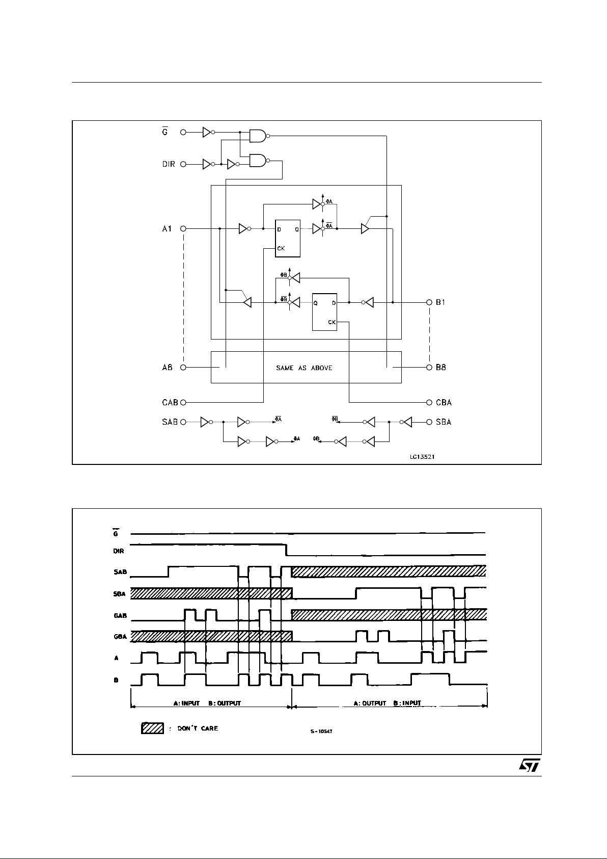
LOGIC DIAGRAM
This log i c diagram has not be used to esti m ate propaga tion delays
TIMING CHART

M74LCX646
5/13
ABSOLUTE MAXIMUM RATIN GS
Absolute Maximum Ratings are those values beyond which damage to the device may occur. Functional operation under these conditions is
not implied
1) I
O
absolute ma xim um rating mu st be observed
2) V
O
< GND
RECOMMENDED OPERATING CONDITIONS
1) Truth T abl e guaranteed: 1.5V to 3.6V
2) V
IN
from 0.8V to 2V at VCC = 3.0V
Symbol Parameter Value Unit
V
CC
Supply Voltage
-0.5 to +7.0 V
V
I
DC Input Voltage
-0.5 to +7.0 V
V
O
DC Output Voltage (OFF State)
-0.5 to +7.0 V
V
O
DC Output Voltage (High or Low State) (note 1) -0.5 to VCC + 0.5
V
I
IK
DC Input Diode Current
- 50 mA
I
OK
DC Output Diode Current (note 2)
- 50 mA
I
O
DC Output Current
± 50 mA
I
CC
DC Supply Current per Supply Pin
± 100 mA
I
GND
DC Ground Current per Supply Pin
± 100 mA
T
stg
Storage Temperature
-65 to +150 °C
T
L
Lead Temperature (10 sec)
300 °C
Symbol Parameter Value Unit
V
CC
Supply Voltage (note 1)
2.0 to 3.6 V
V
I
Input Voltage
0 to 5.5 V
V
O
Output Voltage (OFF State)
0 to 5.5 V
V
O
Output Voltage (High or Low State) 0 to V
CC
V
I
OH
, I
OL
High or Low Level Output Current (VCC = 3.0 to 3.6V)
± 24 mA
I
OH
, I
OL
High or Low Level Output Current (VCC = 2.7V)
± 12 mA
T
op
Operating Temperature
-55 to 125 °C
dt/dv Input Rise and Fall Time (note 2) 0 to 10 ns/V

M74LCX646
6/13
DC SPECIFICATIONS
DYNAMIC SWITCHING CHARACTERISTICS
1) Number of outputs d ef i ned as "n". Me asured with "n-1" output s switching from HIGH to LO W or LOW to HIGH. The remaini ng outpu t is
measur ed i n the LOW state.
Symbol Parameter
Test Condition Value
Unit
V
CC
(V)
-40 to 85 °C -55 to 125 °C
Min. Max. Min. Max.
V
IH
High Level Input
Voltage
2.7 to 3.6
2.0 2.0 V
V
IL
Low Level Input
Voltage
0.8 0.8 V
V
OH
High Level Output
Voltage
2.7 to 3.6
I
O
=-100 µAVCC-0.2 VCC-0.2
V
2.7
I
O
=-12 mA
2.2 2.2
3.0
I
O
=-18 mA
2.4 2.4
I
O
=-24 mA
2.2 2.2
V
OL
Low Level Output
Voltage
2.7 to 3.6
I
O
=100 µA
0.2 0.2
V
2.7
I
O
=12 mA
0.4 0.4
3.0
I
O
=16 mA
0.4 0.4
I
O
=24 mA
0.55 0.55
I
I
Input Leakage
Current
2.7 to 3.6
V
I
= 0 to 5.5V
± 5 ± 5 µA
I
off
Power Off Leakage
Current
0
V
I
or VO = 5.5V
10 10 µA
I
OZ
High Impedance
Output Leakage
Current
2.7 to 3.6
V
I
= VIH or V
IL
VO = 0 to V
CC
± 5 ± 5 µA
I
CC
Quiescent Supply
Current
2.7 to 3.6
VI = VCC or GND
10 10
µA
V
I
or VO= 3.6 to 5.5V
± 10 ± 10
∆I
CC
ICC incr. per Input
2.7 to 3.6
VIH = VCC - 0.6V
500 500 µA
Symbol Parameter
Test Condition Value
Unit
V
CC
(V)
T
A
= 25 °C
Min. Typ. Max.
V
OLP
Dynamic Low Level Quiet
Output (note 1)
3.3
C
L
= 50pF
V
IL
= 0V, VIH = 3.3V
0.8
V
V
OLV
-0.8

M74LCX646
7/13
AC ELECTRICAL CHARACTERISTICS
1) Skew is defined as the absolute value of the difference between the actual propagation delay for any two outputs of the same device switching in the same direction, either HIGH or LOW (t
OSLH
= | t
PLHm
- t
PLHn
|, t
OSHL
= | t
PHLm
- t
PHLn
|)
2) Param eter guaran te ed by design
CAPACITIVE CHARACTERISTICS
1) CPD is defined as the value of the IC’s internal equivalent capacitance which is calculated from the operating current consumption without
load. (Refer to Test Circuit). Average operating current can be obtained by the following equation. I
CC(opr)
= CPD x VCC x fIN + ICC/8 (per c ircuit )
Symbol Parameter
Test Condition Value
Unit
V
CC
(V)
C
L
(pF)
R
L
(Ω)
t
s
= t
r
(ns)
-40 to 85 °C -55 to 125 °C
Min. Max. Min. Max.
t
PLH tPHL
Propagation Delay
Time (CAB or CBA
to An or Bn)
2.7
50 500 2.5
1.5 9.5 1.5 9.5
ns
3.0 to 3.6 1.5 8.5 1.5 8.5
t
PLH tPHL
Propagation Delay
Time (An to Bn or Bn
to An)
2.7
50 500 2.5
1.5 8. 0 1.5 8.0
ns
3.0 to 3.6 1.5 7.0 1.5 7.0
t
PLH tPHL
Propagation Delay
Time (SAB or SBA
to An or Bn)
2.7
50 500 2.5
1.5 9.5 1.5 9.5
ns
3.0 to 3.6 1.5 8.5 1.5 8.5
t
PZL tPZH
Output Enable Time
(G
, DIR to An, Bn)
2.7
50 500 2.5
1.5 9.5 1.5 9.5
ns
3.0 to 3.6 1.5 8.5 1.5 8.5
t
PLZ tPHZ
Output Disable Time
(G
, DIR to An, Bn)
2.7
50 500 2.5
1.5 9.5 1.5 9.5
ns
3.0 to 3.6 1.5 8.5 1.5 8.5
t
S
Setup Time, HIGH or
LOW level Data to
CAB, CBA
2.7
50 500 2.5
2.5 2.5
ns
3.0 to 3.6 2.5 2.5
t
h
Hold Time, HIGH or
LOW level Data to
CAB, CBA
2.7
50 500 2.5
1.5 1.5
ns
3.0 to 3.6 1.5 1.5
t
W
CAB, CBA Pulse
Width, HIGH or
LOW
2.7
50 500 2.5
4.0 4.0
ns
3.0 to 3.6 3.3 3.3
f
MAX
Clock Pulse
Frequency
3.0 to 3.6 50 500 2.5 150 150 MHz
t
OSLH
t
OSHL
Output To Output
Skew Time (note1,
2)
3.0 to 3.6 50 500 2.5 1.0 1.0 ns
Symbol Parameter
Test Condition Value
Unit
V
CC
(V)
T
A
= 25 °C
Min. Typ. Max.
C
IN
Input Capacitance
3.3
VIN = 0 to V
CC
6pF
C
I/O
I/O Capacitance
3.3
VIN = 0 to V
CC
10 pF
C
PD
Power Dissipation Capacitance
(note 1)
3.3 fIN = 10MHz
V
IN
= 0 or V
CC
37
pF

M74LCX646
8/13
TEST CIRCUIT
CL = 50 pF or equival ent (includes jig and probe capacitance)
R
L
= R1 = 500Ω or equivalent
R
T
= Z
OUT
of pulse generator (typically 50Ω)
WAVEFORM 1 : PROPAGATION DELAYS, SAB, SBA, An, Bn, TIMES (f=1MHz; 50% duty cycle)
TEST SWITCH
t
PLH
, t
PHL
Open
t
PZL
, t
PLZ
6V
t
PZH
, t
PHZ
GND

M74LCX646
9/13
WAVEFORM 2 : OUTPUT ENABLE AND DISABLE TIME (f=1MHz; 50% duty cycl e)

M74LCX646
10/13
WAVEFORM 3 : SETUP AND HOLD TIME, CAB, CBA MAXIMUM FREQUENCY (f=1MHz; 50% duty
cycle)
WAVEFORM 4 : PU LSE WIDTH (f=1MHz; 50% duty cycle)

M74LCX646
11/13
DIM.
mm. inch
MIN. TYP MAX. MIN. TYP. MAX.
A 2.65 0.104
a1 0.1 0.2 0.004 0.008
a2 2.45 0.096
b 0.35 0.49 0.014 0.019
b1 0.23 0.32 0.009 0.012
C 0.5 0.020
c1 45° (typ.)
D 15.20 15.60 0.598 0.614
E 10.00 10.65 0.393 0.419
e 1.27 0.050
e3 13.97 0.550
F 7.40 7.60 0.291 0.300
L 0.50 1.27 0.020 0.050
S8° (max.)
SO-24 MECHANICAL DATA
PO13T
F
C
L
E
a1
b1
A
e
D
e3
b
24 13
112
c1
s
a2

M74LCX646
12/13
DIM.
mm. inch
MIN. TYP MAX. MIN. TYP. MAX.
A 1.1 0.043
A1 0.05 0.15 0.002 0.006
A2 0.9 0.035
b 0.19 0.30 0.0075 0.0118
c 0.09 0.20 0.0035 0.0079
D 7.7 7.9 0.303 0.311
E 6.25 6.5 0.246 0.256
E1 4.3 4.5 0.169 0.177
e 0.65 BSC 0.0256 BSC
K0° 8°0° 8°
L 0.50 0.70 0.020 0.028
TSSOP24 MECHANICAL DATA
c
E
b
A2
A
E1
D
1
PIN 1 IDENTIFICATION
A1
L
K
e
7047476A

M74LCX646
Information furnished is bel ieved to be accurate and reliable. However, STMicroe lectronics assumes no responsibility for the
consequences of use of such information nor for any infringement of patents or other rights of third parties which may result from
its use. No li cense is granted by imp lication or otherwise under a ny patent or patent rig hts of STMicroelectronics. Specificat ions
mentioned in this publication ar e subject to change without notice. This publication supersedes and replaces all information
previously supplied. S TMicroelectronics products are not authorized for use as critica l components in life suppo rt devices or
systems without express written approval of STMicroelectronics.
© The ST logo is a registered trademark of STMicroelectronics
© 2001 STM icroelectronics - Pri n ted in Italy - All Rights Reser ved
STMicr o el ectronics GROUP OF COMPANI ES
Australi a - Brazil - China - Finland - F rance - Germany - Hong Kon g - India - Italy - Japan - Malaysi a - Malta - Morocco
Singapo re - Spain - Swe den - Switze rl and - United K i ngdom
© http://www.st.com
13/13
 Loading...