

1/10September 2001
■ 5V TOLERANT INPUTS AND OUTPUTS
■ HIGH SPEED :
f
MAX
= 150 MHz (MIN.) at VCC = 3V
■ POWER DOWN PROTECTI ON ON INPUTS
AND OUTPUTS
■ SYMMETRICAL OUTPUT IMPEDANCE:
|I
OH
| = IOL = 24mA (MIN) at VCC = 3V
■ PCI BUS LEVELS GUARANT EED AT 24 mA
■ BALANCED PROPAGATION DELAYS:
t
PLH
≅ t
PHL
■ OPERATING VOLTAGE RANGE:
V
CC
(OPR) = 2.0V to 3.6V (1.5V Data
Retention)
■ PIN AND FUNCTION COMPATIBLE WITH
74 SERIES 574
■ LATCH-UP PERFORMANCE EXCEEDS
500mA (JESD 17)
■ ESD PERFORMANCE:
HBM > 2000V (MIL STD 883 method 3015);
MM > 200V
DESCRIPTION
The 74LCX574 is a low voltage CMOS OCTAL
D-TYPE FLIP FLOP with 3 STATE OUTPUT
NON-INVERTING fabricated with sub-micron
silicon gate and double-layer metal wiring C
2
MOS
technology. It is ideal for low power and high
speed 3.3V applications; it can be interfaced to 5V
signal environment for both inputs and outputs.
These 8 bit D-Type flip-flops are controlled by a
clock input (CK) and an output enable input (OE
).
On the positive transition of the clock, the Q
outputs will be set to the logic state that were
setup at the D inputs.
While the (OE
) input is low, the 8 outputs will be in
a normal logic state (high or low logic level) and
while high level the outputs will be in a high
impedance state.
The Output control does not affect the internal
operation of flip flops; that is, the old data can be
retained or the new data can be entered even
while the outputs are off.
It has same speed performance at 3. 3V than 5V
AC/ACT family, combined with a lower power
consumption.
All inputs and outputs are equipped with
protection circuits against stat ic discharge, giving
them 2KV ESD immunity and transient excess
voltage.
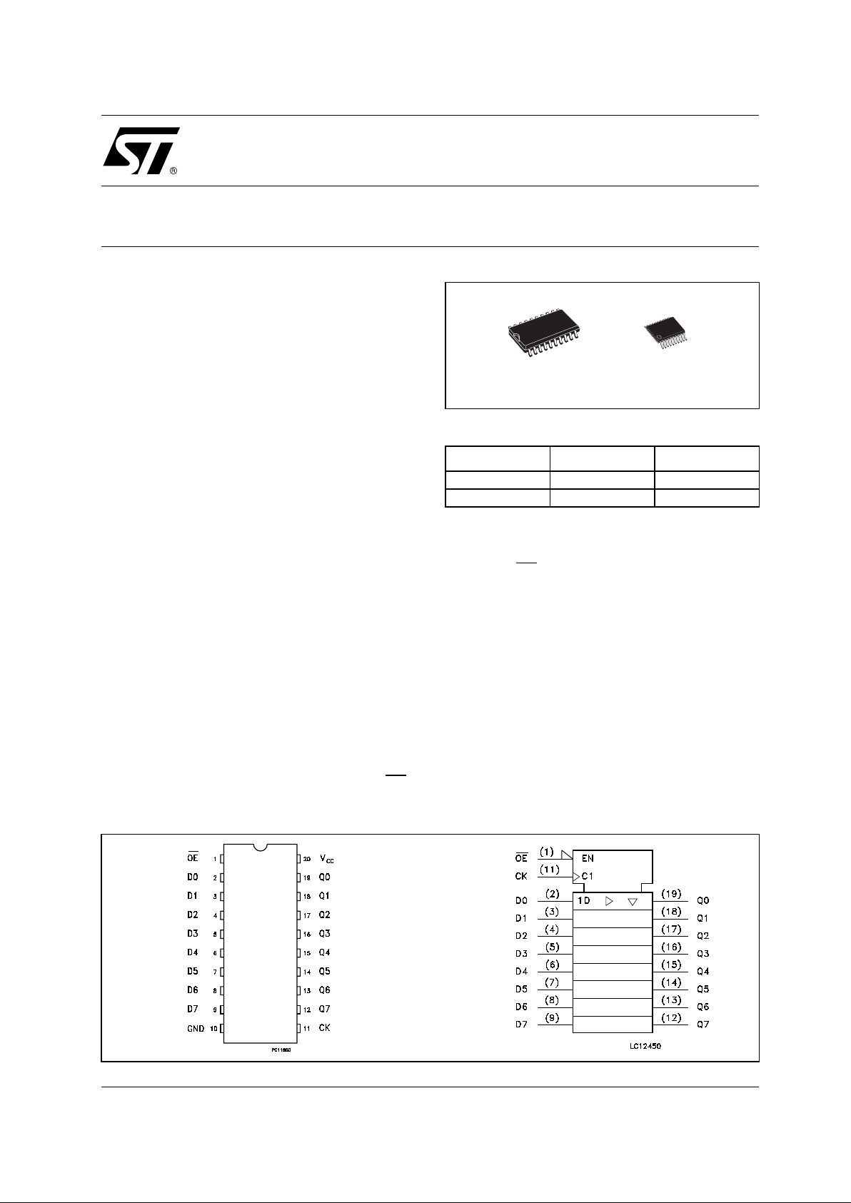
74LCX574
OCTAL D-TYPE FLIP FLOP NON-INVERTING (3-STATE)
WITH 5V TOLERANT INPUTS AND OUTPUTS
PIN CONNECTION AND IEC LOGIC SYMBOLS
ORDER CODES
PACKAGE TUBE T & R
SOP 74LCX574M 74LCX574MTR
TSSOP 74LCX574TTR
TSSOPSOP
74LCX574
2/10
INPUT AND OUTPUT EQUIVALENT CIRCUIT
PIN DESCRIPTION TRUTH TABLE
X : Don’t Care
Z : High Impedance
LOGIC DIAGRAM
This log i c diagram has not be used to esti m ate propaga tion delays
PIN No SYMBOL NAME AND FUNCTION
1OE
3-State Output Enable
Input (Active LOW)
2, 3, 4, 5, 6,
7, 8, 9
D0 to D7 Data Inputs
12, 13, 14,
15, 16, 17,
18, 19
Q0 to Q7 3-State Outputs
1 1 CK Clock Input (LOW-to-HIGH
Edge Triggered)
10 GND Ground (0V)
20 V
CC
Positive Supply Voltage
INPUT OUTPUT
OE
CK D Q
HXX Z
L X NO CHANGE
LLL
LHH
74LCX574
3/10
ABSOLUTE MAXIMUM RATINGS
Absolute Maximum Ratings are those values beyond which damage to the device may occur. Functional operation under these conditions is
not implied
1) I
O
absolute ma xim um rating mu st be observed
2) V
O
< GND
RECOMMENDED OPERATING CONDITIONS
1) Truth T abl e guaranteed: 1.5V to 3.6V
2) V
IN
from 0.8V to 2V at VCC = 3.0V
Symbol Parameter Value Unit
V
CC
Supply Voltage
-0.5 to +7.0 V
V
I
DC Input Voltage
-0.5 to +7.0 V
V
O
DC Output Voltage (OFF State)
-0.5 to +7.0 V
V
O
DC Output Voltage (High or Low State) (note 1) -0.5 to VCC + 0.5
V
I
IK
DC Input Diode Current
- 50 mA
I
OK
DC Output Diode Current (note 2)
- 50 mA
I
O
DC Output Current
± 50 mA
I
CC
DC Supply Current per Supply Pin
± 100 mA
I
GND
DC Ground Current per Supply Pin
± 100 mA
T
stg
Storage Temperature
-65 to +150 °C
T
L
Lead Temperature (10 sec)
300 °C
Symbol Parameter Value Unit
V
CC
Supply Voltage (note 1)
2.0 to 3.6 V
V
I
Input Voltage
0 to 5.5 V
V
O
Output Voltage (OFF State)
0 to 5.5 V
V
O
Output Voltage (High or Low State) 0 to V
CC
V
I
OH
, I
OL
High or Low Level Output Current (VCC = 3.0 to 3.6V)
± 24 mA
I
OH
, I
OL
High or Low Level Output Current (VCC = 2.7V)
± 12 mA
T
op
Operating Temperature
-55 to 125 °C
dt/dv Input Rise and Fall Time (note 2) 0 to 10 ns/V

74LCX574
4/10
DC SPECIFICATIONS
DYNAMIC SWITCHING CHARACTERISTICS
1) Number of outputs d ef i ned as "n". Me asured with "n-1" output s switching from HIGH to LO W or LOW to HIGH. The remaini ng outpu t is
measur ed i n the LOW state.
Symbol Parameter
Test Condition Value
Unit
V
CC
(V)
-40 to 85 °C -55 to 125 °C
Min. Max. Min. Max.
V
IH
High Level Input
Voltage
2.7 to 3.6
2.0 2.0 V
V
IL
Low Level Input
Voltage
0.8 0.8 V
V
OH
High Level Output
Voltage
2.7 to 3.6
I
O
=-100 µAVCC-0.2 VCC-0.2
V
2.7
I
O
=-12 mA
2.2 2.2
3.0
I
O
=-18 mA
2.4 2.4
I
O
=-24 mA
2.2 2.2
V
OL
Low Level Output
Voltage
2.7 to 3.6
I
O
=100 µA
0.2 0.2
V
2.7
I
O
=12 mA
0.4 0.4
3.0
I
O
=16 mA
0.4 0.4
I
O
=24 mA
0.55 0.55
I
I
Input Leakage
Current
2.7 to 3.6
V
I
= 0 to 5.5V
± 5 ± 5 µA
I
off
Power Off Leakage
Current
0
V
I
or VO = 5.5V
10 10 µA
I
OZ
High Impedance
Output Leakage
Current
2.7 to 3.6
V
I
= VIH or V
IL
VO = 0 to V
CC
± 5 ± 5 µA
I
CC
Quiescent Supply
Current
2.7 to 3.6
VI = VCC or GND
10 10
µA
V
I
or VO= 3.6 to 5.5V
± 10 ± 10
∆I
CC
ICC incr. per Input
2.7 to 3.6
VIH = VCC - 0.6V
500 500 µA
Symbol Parameter
Test Condition Value
Unit
V
CC
(V)
T
A
= 25 °C
Min. Typ. Max.
V
OLP
Dynamic Low Level Quiet
Output (note 1)
3.3
C
L
= 50pF
V
IL
= 0V, VIH = 3.3V
0.8
V
V
OLV
-0.8

74LCX574
5/10
AC ELECTRICAL CHARACTERISTICS
1) Skew is defined as the absolute value of the difference between the actual propagation delay for any two outputs of the same device switching in the same direction, either HIGH or LOW (t
OSLH
= | t
PLHm
- t
PLHn
|, t
OSHL
= | t
PHLm
- t
PHLn
|)
2) Param eter guaran te ed by design
CAPACITIVE CHARACTERISTICS
1) CPD is defined as the value of the IC’s internal equivalent capacitance which is calculated from the operating current consumption without
load. (R ef er to Test Circui t). Averag e operating cu rrent can be obtained by the foll owing equat io n. I
CC(opr)
= CPD x VCC x fIN + ICC/8 (per
flip-flop)
Symbol Parameter
Test Condition Value
Unit
V
CC
(V)
C
L
(pF)
R
L
(Ω)
t
s
= t
r
(ns)
-40 to 85 °C -55 to 125 °C
Min. Max. Min. Max.
t
PLH tPHL
Propagation Delay
Time
2.7
50 500 2.5
1.5 9. 5 1.5 9.5
ns
3.0 to 3.6 1.5 8.5 1.5 8.5
t
PZL tPZH
Output Enable Time
to HIGH and LOW
level
2.7
50 500 2.5
1.5 9. 5 1.5 9.5
ns
3.0 to 3.6 1.5 8.5 1.5 8.5
t
PLZ tPHZ
Output Disable Time
from HIGH to LOW
level
2.7
50 500 2.5
1.5 8.5 1.5 8.5
ns
3.0 to 3.6 1.5 7.5 1.5 7.5
t
S
Set-Up Time, HIGH
or LOW level
(Dn to CK)
2.7
50 500 2.5
2.5 2.5
ns
3.0 to 3.6 2.5 2.5
t
h
Hold Time, HIGH or
LOW level
(Dn to CK)
2.7
50 500 2.5
1.5 1.5
ns
3.0 to 3.6 1.5 1.5
t
W
CK Pulse Width,
HIGH or LOW
2.7
50 500 2.5
3.3 3.3
ns
3.0 to 3.6 3.3 3.3
f
MAX
Clock Pulse
Frequency
3.0 to 3.6 50 500 2.5 165 150 MHz
t
OSLH
t
OSHL
Output To Output
Skew Time (note1,
2)
3.0 to 3.6 50 500 2.5 1.0 1.0 ns
Symbol Parameter
Test Condition Value
Unit
V
CC
(V)
T
A
= 25 °C
Min. Typ. Max.
C
IN
Input Capacitance
3.3
VIN = 0 to V
CC
6pF
C
OUT
Output Capacitance
3.3
VIN = 0 to V
CC
12 pF
C
PD
Power Dissipation Capacitance
(note 1)
3.3 fIN = 10MHz
V
IN
= 0 or V
CC
25
pF
74LCX574
6/10
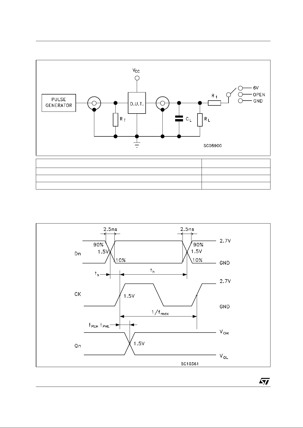
TEST CIRCUIT
CL = 50 pF or equival ent (includes jig and probe capacitance)
R
L
= R1 = 500Ω or equivalent
R
T
= Z
OUT
of pulse generator (typically 50Ω)
WAVEFORM 1 : PROPAGATION DELAYS, SETUP AND HOLD TIMES, MAXIMUM CK FREQUENCY
(f=1MHz; 50% duty cycle)
TEST SWITCH
t
PLH
, t
PHL
Open
t
PZL
, t
PLZ
6V
t
PZH
, t
PHZ
GND

74LCX574
7/10
WAVEFORM 2 : OUTPUT ENABLE AND DISABLE TIMES (f=1MHz; 50% duty cycle)
WAVEFORM 3 : PULSE WIDTH (f=1MHz; 50% duty cycle)

74LCX574
8/10
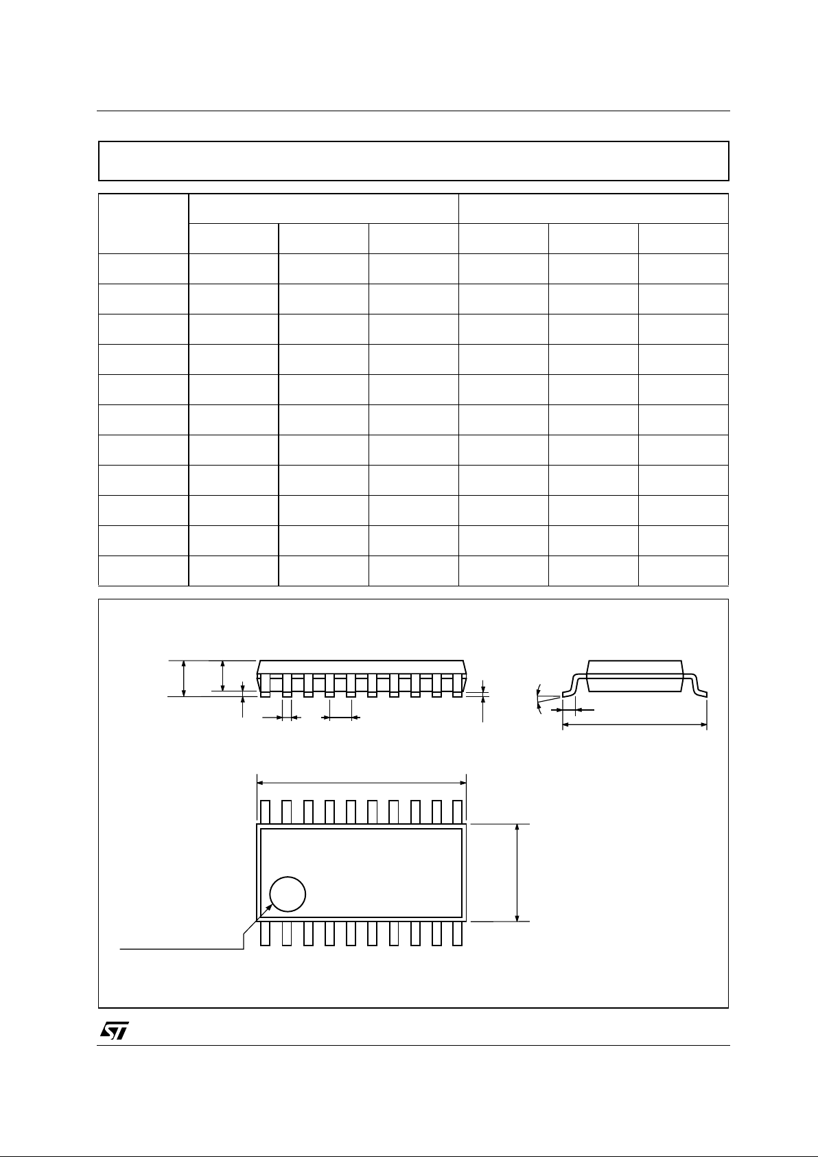
DIM.
mm. inch
MIN. TYP MAX. MIN. TYP. MAX.
A 2.65 0.104
a1 0.1 0.2 0.004 0.008
a2 2.45 0.096
b 0.35 0.49 0.014 0.019
b1 0.23 0.32 0.009 0.012
C 0.5 0.020
c1 45° (typ.)
D 12.60 13.00 0.496 0.512
E 10.00 10.65 0.393 0.419
e 1.27 0.050
e3 11.43 0.450
F 7.40 7.60 0.291 0.300
L 0.50 1.27 0.020 0.050
M 0.75 0.029
S8° (max.)
SO-20 MECHANICAL DATA
PO13L
74LCX574
9/10
DIM.
mm. inch
MIN. TYP MAX. MIN. TYP. MAX.
A 1.2 0.047
A1 0.05 0.15 0.002 0.004 0.006
A2 0.8 1 1.05 0.031 0.039 0.041
b 0.19 0.30 0.007 0.012
c 0.09 0.20 0.004 0.0089
D 6.4 6.5 6.6 0.252 0.256 0.260
E 6.2 6.4 6.6 0.244 0.252 0.260
E1 4.3 4.4 4.48 0.169 0.173 0.176
e 0.65 BSC 0.0256 BSC
K0° 8°0° 8°
L 0.45 0.60 0.75 0.018 0.024 0.030
TSSOP20 MECHANICAL DATA
c
E
b
A2
A
E1
D
1
PIN 1 IDENTIFICATION
A1
L
K
e
0087225C

74LCX574
10/10
Information furnished is bel ieved to be accurate and reliable. However, STMicroe lectronics assumes no responsibility for the
consequences of use of such information nor for any infringement of patents or other rights of third parties which may result from
its use. No li cense is granted by imp lication or otherwise under a ny patent or patent rig hts of STMicroelectronics. Specificat ions
mentioned in this publication ar e subject to change without notice. This publication supersedes and replaces all information
previously supplied. S TMicroelectronics products are not authorized for use as critica l components in life suppo rt devices or
systems without express written approval of STMicroelectronics.
© The ST logo is a registered trademark of STMicroelectronics
© 2000 STM icroelectronics - Pri n ted in Italy - All Rights Reser ved
STMicr o el ectronics GROUP OF COMPANI ES
Australi a - Brazil - China - Finland - F rance - Germany - Hong Kon g - India - Italy - Japan - Malaysi a - Malta - Morocco
Singapo re - Spain - Swe den - Switze rl and - United K i ngdom
© http://www.st.com
 Loading...