

74LCX373
OCTAL D-TYPE LATCH NON-INVERTING (3-STATE)
WITH 5V TOLERANT INPUTS AND OUTPUTS
■ 5V TOLERANT INPUTS AND OUTPUTS
■ HIGH SPEED :
= 8.0 ns (MAX.) at VCC = 3V
t
PD
■ POWER DOWN PROTECTION ON INPUT S
AND OUTPUTS
■ SYMMETRICAL OUTPUT IMPEDANCE:
| = IOL = 24mA (MIN) at VCC = 3V
|I
OH
■ PCI BUS LEVELS GUARANT EED AT 2 4 mA
■ BALANCED PROPAGATION DELAYS:
t
≅ t
PLH
■ OPERATING VOLTAGE RANGE:
V
CC
PHL
(OPR) = 2.0V to 3.6V (1.5V Data
Retention)
■ PIN AND FUNCTION COMPATIBLE WITH
74 SERIES 373
■ LATCH-UP PERFORMANCE EXCEEDS
500mA (JESD 17)
■ ESD PERFORMANCE:
HBM > 2000V (MIL STD 883 method 3015);
MM > 200V
DESCRIPTION
The 74LCX373 is a low voltage CMOS OCTAL
D-TYPE LATCH with 3 STATE OUTPUT
NON-INVERTING fabricated with sub-micron
silicon gate and double-layer metal wiring C
2
MOS
technology. It is ideal for low power and high
speed 3.3V applications; it can be interfaced to 5V
signal environment for both inputs and outputs.
These 8 bit D-Type latch are controlled by a latch
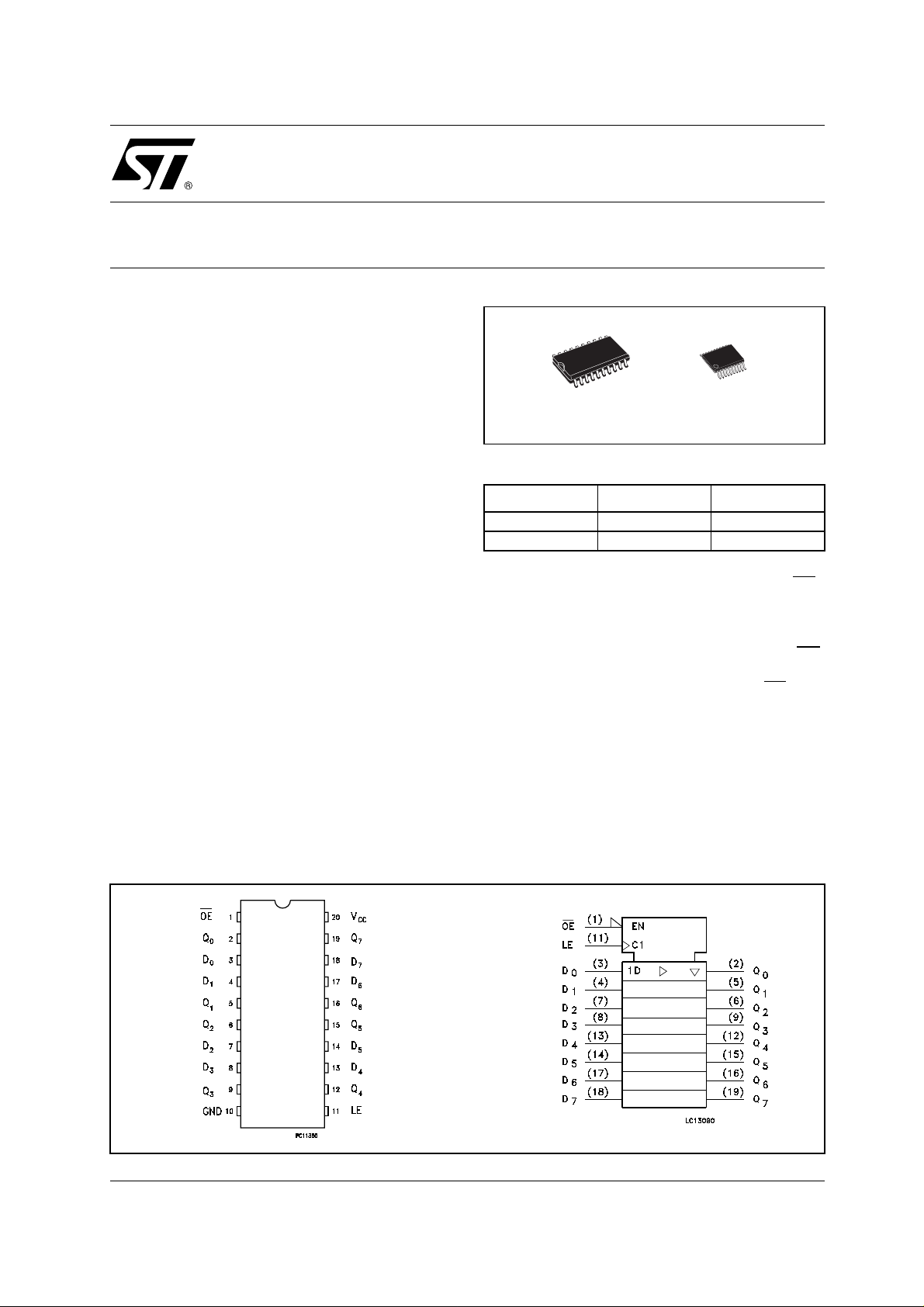
PIN CONNECTION AND IEC LOGIC SYMBOLS
TSSOPSOP
ORDER CODES
PACKAGE TUBE T & R
SOP 74LCX373M 74LCX373MTR
TSSOP 74LCX373TTR
enable input (LE) and an output enable input (OE
While the LE inputs is held at a high level, t he Q
outputs will follow the data input. When the LE is
taken low, the Q outputs will be latched precisely
at the logic level of D input data. While the (OE
input is low, the 8 outputs will be in a normal lo gic
state (high or low logic level ) and while (OE
) is in
high leve l, the o utputs will be in a hig h imp edance
state.
It has same speed performance at 3. 3V than 5V
AC/ACT family, combined with a lower power
consumption.
All inputs and outputs are equipped with
protection circuits against stat ic discharge, giving
them 2KV ESD immunity and transient excess
voltage.
).
)
1/10September 2001

74LCX373
INPUT AND OUTPUT EQUIVALENT CIRCUIT
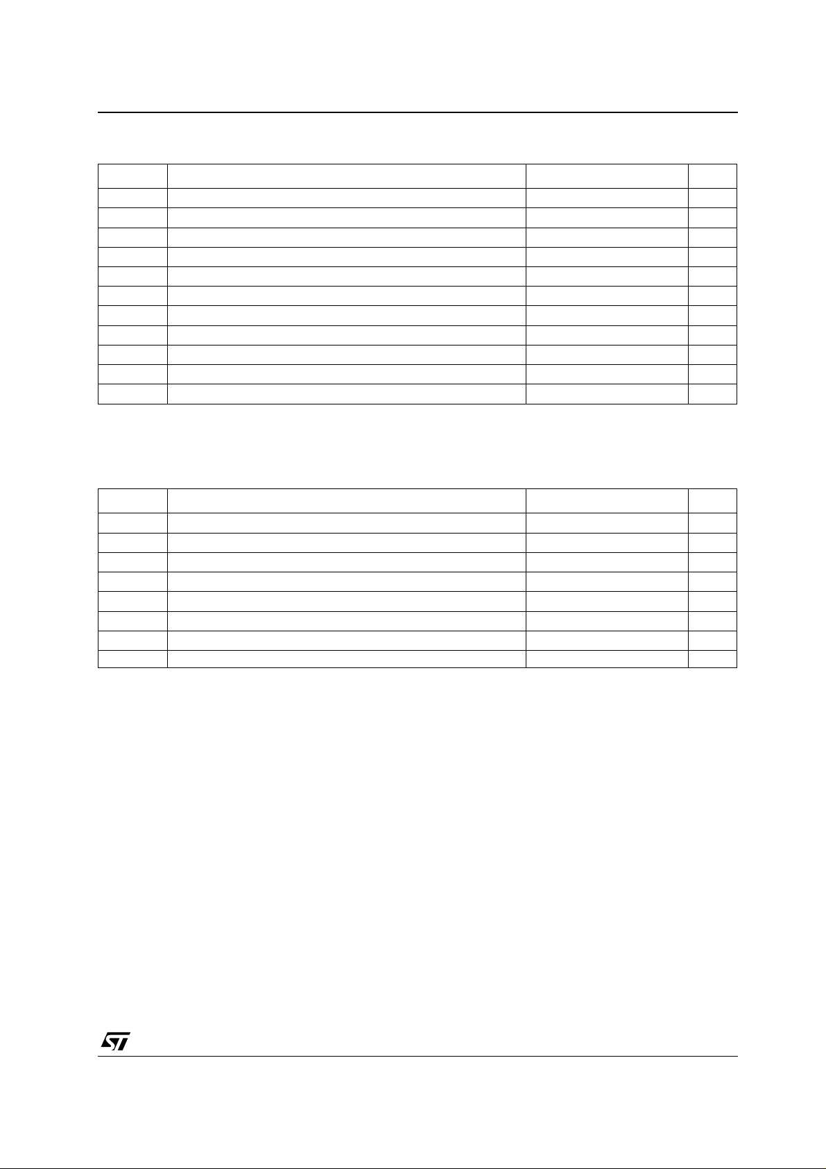
PIN DESCRIPTION TRUTH TABLE
PIN No SYMBOL NAME AND FUNCTION
1OE
3 State Output Enable
Input (Active LOW)
2, 5, 6, 9, 12,
D0 to D7 Data Inputs
15, 16,19
3, 4, 7, 8, 13,
Q0 to Q7 3-State Outputs
14, 17, 18
11 LE Latch Enable Input
10 GND Ground (0V)
20 V
CC
Positive Supply Voltage
LOGIC DIAGRAM
INPUT OUTPUT
OE
LE D Q
HXX Z
L L X NO CHANGE*
LHL L
LHH H
X : Don’t Care
Z : High Impedance
* : Q Outputs are latched at the time when th e LE input is taken
LOW.
This log i c diagram has not be used to esti m ate propaga tion delays
2/10
74LCX373
ABSOLUTE MAXIMUM RATINGS
Symbol Parameter Value Unit
V
V
V
V
I
I
OK
I
I
CC
I
GND
T
T
Absolute Maximum Ratings are those values beyond which damage to the device may occur. Functional operation under these conditions is
not implied
1) I
absolute ma xim um rating mu st be observed
O
2) V
< GND
O
RECOMMENDED OPERATING CONDITIONS
Symbol Parameter Value Unit
V
V
V
V
I
OH
I
OH
T
dt/dv Input Rise and Fall Time (note 2) 0 to 10 ns/V
1) Truth T abl e guaranteed: 1.5V to 3.6V
2) V
from 0.8V to 2V at VCC = 3.0V
IN
Supply Voltage
CC
DC Input Voltage
I
DC Output Voltage (OFF State)
O
DC Output Voltage (High or Low State) (note 1) -0.5 to VCC + 0.5
O
DC Input Diode Current
IK
DC Output Diode Current (note 2)
DC Output Current
O
DC Supply Current per Supply Pin
DC Ground Current per Supply Pin
Storage Temperature
stg
Lead Temperature (10 sec)
L
Supply Voltage (note 1)
CC
Input Voltage
I
Output Voltage (OFF State)
O
Output Voltage (High or Low State) 0 to V
O
, I
High or Low Level Output Current (VCC = 3.0 to 3.6V)
OL
, I
High or Low Level Output Current (VCC = 2.7V)
OL
Operating Temperature
op
-0.5 to +7.0 V
-0.5 to +7.0 V
-0.5 to +7.0 V
- 50 mA
- 50 mA
± 50 mA
± 100 mA
± 100 mA
-65 to +150 °C
300 °C
2.0 to 3.6 V
0 to 5.5 V
0 to 5.5 V
CC
± 24 mA
± 12 mA
-55 to 125 °C
V
V
3/10
 Loading...