


74LCX16373
LOW VOLTAGE CMOS 16-BIT D-TYPE LATCH (3-STATE)
WITH 5V TOLERANT INPUTS AND OUTPUTS
■ 5V TOLERANT INPUTS AND OUTPUTS
■ HIGH SPEED :
t
= 5.4 ns (MAX.) at VCC=3V
PD
■ POWER DOWN PROTECTION ON INPUTS
AND OUTPUTS
■ SYMMETRICAL OUTPUT IMPEDANCE:
|I
|=IOL= 24mA (MIN) at VCC=3V
OH
■ PCI BUS LEVELS GUARANTEED AT 24 mA
■ BALANCED PROPAGATION DELAYS:
t
≅ t
PLH
PHL
■ OPERATING VOLTAGE RAN GE:
V
(OPR) = 2.0V to 3.6V (1.5V D ata
CC
Retention)
■ PIN AND FUNCTION COMPATIBLE WITH
74 SERIES 16373
■ LATCH-UP PERFORMANCE EXCEEDS
500mA (JESD 17)
■ ESD PERFORMANCE:
HBM > 2000V (MIL STD 883 method 3015);
MM > 200V
ORDER CODES
PACKAGE TUBE T & R
TSSOP 74LCX16373TTR
PIN CO NNE CTION
TSSOP
DESCRIPTION
The 74LCX16373 is a low voltage CMOS 16 BIT
D-TYPE LATCH with 3 STATE OUTPUTS NON
INVERTING fabricated with sub-micron silicon
gate and double-layer metal wiring C
2
MOS
technology. It is ideal for low power and hi gh
speed 3. 3V applications; it can be interfaced to 5V
signal environment for both inputs and outputs.
These 16 bit D-TYPE latches are byte controlled
by two latch enable inputs (nLE) and two output
enable inputs(OE
).
While the nLE input is held at a high level, the nQ
outputs will follow the data input precisely.
When the nLE is taken LOW, the nQ outputs will
be latched precisely at the logic level of D input
data.
While the (nOE
) input is low, the nQ outputs wi ll be
in a normal logic state (high or low logic level) and
while high levelthe outputs w ill be in a high impedance state.
It has same speed performance at 3.3V than 5V
AC/ACT family, com bined with a lower power
consumption.
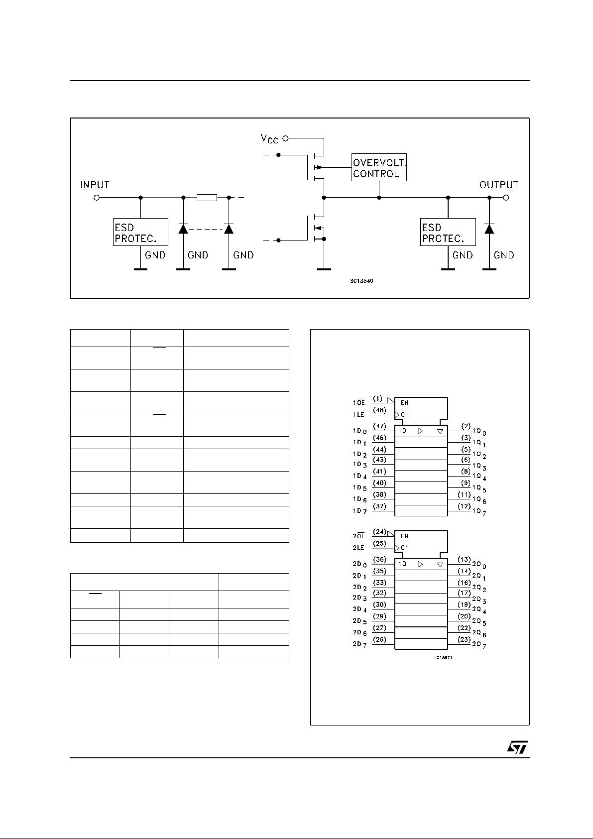
All inputs and outputs are equipped with prot ec tion circuits against static disc harge, giving them
2KV ESD immunity and transient excess vo ltage.
1/10February 2003
74LCX16373
INPUT AND OUTPUT EQUIVALENT CIRCUIT
PIN DESCRIPTION
PIN No SYMBOL NAME AND FUNCTION
1 1OE
2, 3,5,6,8,9,
11, 12
13,14,16, 17,
19, 20, 22, 23
24 2OE
25 2LE Latch Enable Input
36,35,33, 32,
30, 29, 27, 26
47,46,44, 43,
41, 40, 38, 37
48 1LE Latch Enable Input
4, 10, 15, 21,
28, 34, 39, 45
7, 18, 31, 42 V
1Q0 to 1Q7 3-State Outputs
2Q0 to 2Q7 3-State Outputs
2D0 to 2D7 Data Inputs
1D0 to 1D7 Data Inputs
GND Ground (0V)
CC
3 State Output Enable
Input (Active LOW)
3 State Output Enable
Input (Active LOW)
Positive Supply Voltage
TRUTH TABLE
INPUTS OUTPUT
OE
HXX Z
L L X NO CHANGE *
LHL L
LHH H
X : Don‘t Care
Z : High Impedance
* : Q outputs arelatched atthetime whentheLE inputis taken low
logiclevel.
LE D Q
IEC LOGIC SYMBOLS
2/10
74LCX16373
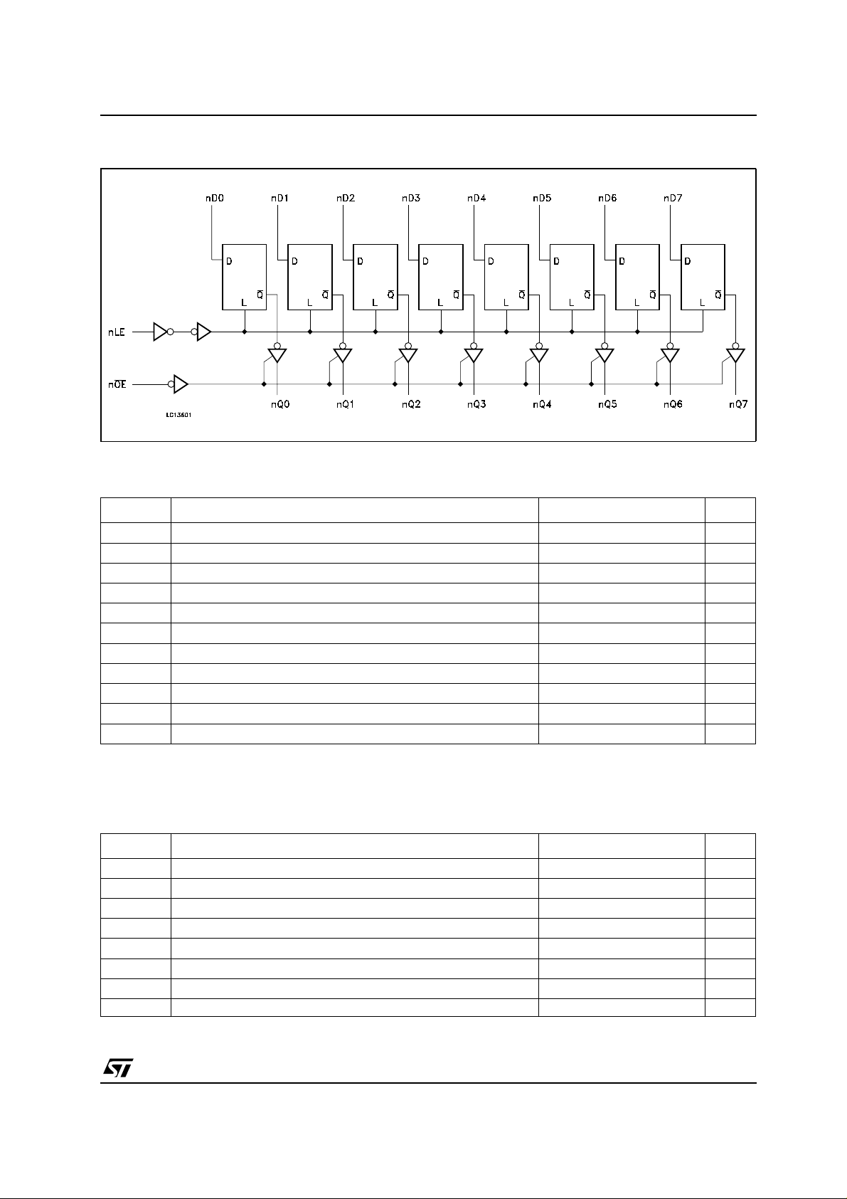
LOGIC DIAGRAM
This logic diagram has not to be used to estimate propagation delays
ABSOLUTE MAXIMUM RATINGS
Symbol Parameter Value Unit
V
V
V
V
I
I
OK
I
I
CC
I
GND
T
T
Absolute Maximum Ratings are those values beyond which damage tothe device may occur. Functional operation under these conditions is
not implied
absolute maximum rating must be observed
1) I
O
<GND
2) V
O
Supply Voltage
CC
DC Input Voltage
I
DC Output Voltage (OFF State)
O
DC Output Voltage (High or Low State) (note 1) -0.5 to VCC+ 0.5
O
DC Input Diode Current
IK
DC Output Diode Current (note 2)
DC Output Current
O
DC Supply Current per Supply Pin
DC Ground Current per Supply Pin
Storage Temperature
stg
Lead Temperature (10 sec)
L
-0.5 to +7.0 V
-0.5 to +7.0 V
-0.5 to +7.0 V
V
-50 mA
-50 mA
± 50 mA
± 100 mA
± 100 mA
-65 to +150 °C
300 °C
RECOMMENDED OPERATING CONDITIONS
Symbol Parameter Value Unit
V
V
V
V
I
OH,IOL
I
OH,IOL
T
dt/dv Input Rise and Fall Time (note 2) 0 to 10 ns/V
1) Truth Table guaranteed: 1.5V to 3.6V
from0.8V to 2Vat VCC=3.0V
2) V
IN
Supply Voltage (note 1)
CC
Input Voltage
I
Output Voltage (OFF State)
O
Output Voltage (High or Low State) 0 to V
O
High or Low Level Output Current (VCC= 3.0 to 3.6V)
High or Low Level Output Current (VCC= 2.7V)
Operating Temperature
op
2.0 to 3.6 V
0 to 5.5 V
0 to 5.5 V
CC
± 24 mA
± 12 mA
-55 to 125 °C
V
3/10
 Loading...