

SGS Thomson Microelectronics 74LCX162541TTR Datasheet
LOW VOLTAGE CMOS 16-BIT BUS BUFFER (3-STATE)
WITH 5V TOLERANT INPUTS AND OUTPUTS
■ 5V TOLERANT INPUTS AND OUTPUTS
■ HIGH SPEED :
t
= 4.4 ns (MAX.) at VCC=3V
PD
■ POWER DOWN PROTECTION ON INPUTS
AND OUTPUTS
■ SYMMETRICAL OUTPUT IMPEDANCE:
|I
|=IOL= 12mA (MIN) at VCC=3V
OH
■ PCI BUS LEVELS GUARANTEED AT 12 mA
■ BALANCED PROPAGATION DELAYS:
t
≅ t
PLH
PHL
■ 26Ω SERIE RESISTORS IN OUTPUTS
■ OPERATING VOLTAGE RANGE:
V
(OPR) = 2.0V to 3.6V (1.5V Data
CC
Retention)
■ PIN AND FUNCTION COMPATIBLE WITH
74 SERIES 162541
■ LATCH-UP PERFORMANCE EXCEEDS
500mA (JESD 17)
■ ESD PERFORMANCE:
HBM > 2000V (MIL STD 883 method 3015);
MM > 200V
74LCX162541
TSSOP
ORDER CODES
PACKAGE TUBE T & R
TSSOP 74LCX162541TTR
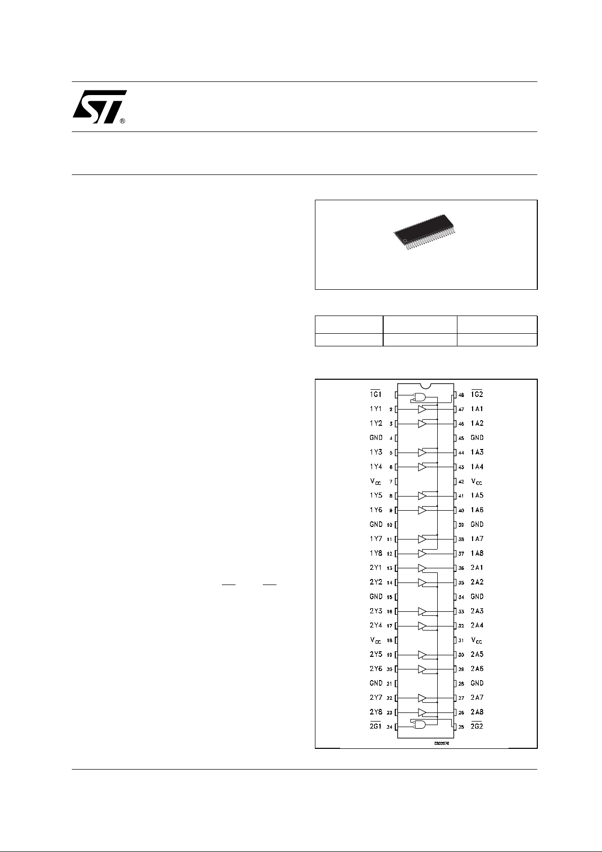
PIN CO NNE CTION
DESCRIPTION
The 74LCX162541 is a low voltage CMOS 16 BIT
BUS BUFFER (NON-INVERTED) fabricated with
sub-micron silicon gate and double-layer metal
wiring C
2
MOS technology. It is ideal for low power
and high speed 3.3V applications; it can be
interfaced to 5V signal environment for both inputs
and outputs.
This is composed of two 8-bit sections with separate output-enable signals. For either 8-bit buffers
section, the 3 STATE control gate operates as a
two input AND such that if eith er nG1
and nG2 are
high, all outputs are in the high impedence state.
This device is designed to be used with 3 state
memory address drivers, etc.
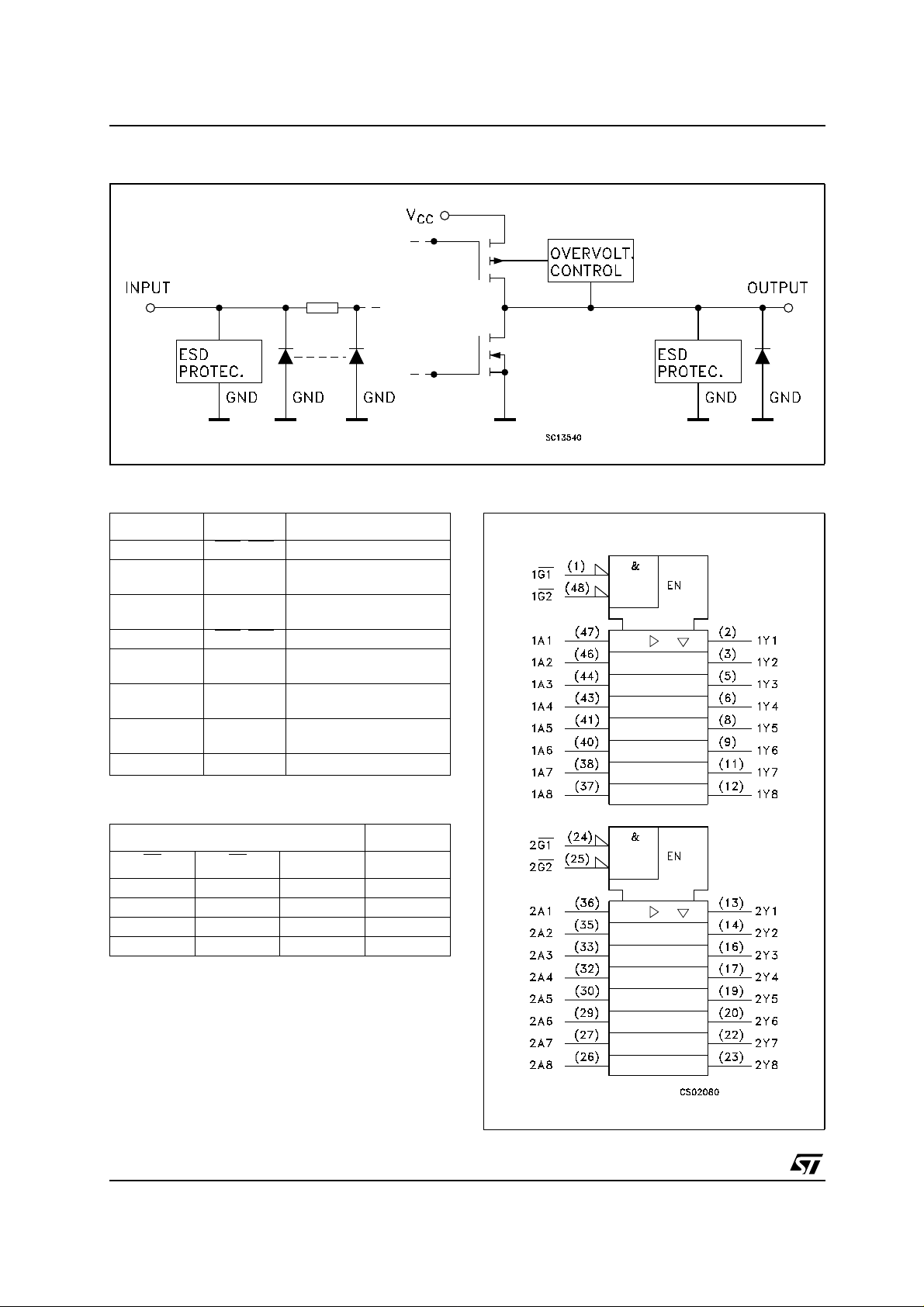
The device circuits is including 26Ω series resistance in the outputs. These resistors permit to reduce line noise in high speed applications.
All inputs and outpu ts are equipped with protection circuits against static discharge, giving them
2KV ESD immunity and transient excess vo ltage.
1/10February 2003
74LCX162541
INPUT AND OUTPUT EQUIVALENT CIRCUIT
PIN DESCRIPTION
PIN No SYMBOL NAME AND FUNCTION
1, 48 1G1
2, 3,5,6,8,9,
11, 12
13,14, 16,17,
19, 20, 22, 23
24, 25 2G1
36,35, 33,32,
30, 29, 27, 26
47,46, 44,43,
41, 40, 38, 37
4, 10, 15, 21,
28, 34, 39, 45
7, 18, 31, 42 V
,1G2 Output Enable Inputs
1Y1 to 1Y8 Data Outputs
2Y1 to 2Y8 Data Outputs
,2G2 Output Enable Inputs
2A1 to 2A8 Data Outputs
1A1 to 1A8 Data Outputs
GND Ground (0V)
CC
Positive Supply Voltage
TRUTH TABLE
INPUTS OUTPUT
G1
HXXZ
XHXZ
LLHH
LLLL
X : Don‘t Care
Z : High Impedance
G2 An Yn
IEC LOGIC SYMBOLS
2/10
74LCX162541
ABSOLUTE MAXIMUM RATINGS
Symbol Parameter Value Unit
V
V
V
V
I
I
OK
I
I
CC
I
GND
T
T
Absolute Maximum Ratings are those values beyond which damage to the device may occur. Functional operation under these conditions is
not implied
1) I
absolute maximum rating must be observed
O
2) VO<GND
RECOMMENDED OPERATING CONDITIONS
Symbol Parameter Value Unit
V
V
V
V
I
OH,IOL
I
OH,IOL
T
dt/dv Input Rise and Fall Time (note 2) 0 to 10 ns/V
1) Truth Table guaranteed: 1.5V to 3.6V
from0.8Vto 2V at VCC=3.0V
2) V
IN
Supply Voltage
CC
DC Input Voltage
I
DC Output Voltage (OFF State)
O
DC Output Voltage (High or Low State) (note 1) -0.5 to VCC+ 0.5
O
DC Input Diode Current
IK
DC Output Diode Current (note 2)
DC Output Current
O
DC Supply Current per Supply Pin
DC Ground Current per Supply Pin
Storage Temperature
stg
Lead Temperature (10 sec)
L
Supply Voltage (note 1)
CC
Input Voltage
I
Output Voltage (OFF State)
O
Output Voltage (High or Low State) 0 to V
O
High or Low Level Output Current (VCC= 3.0 to 3.6V)
High or Low Level Output Current (VCC= 2.7V )
Operating Temperature
op
-0.5 to +7.0 V
-0.5 to +7.0 V
-0.5 to +7.0 V
V
-50 mA
-50 mA
± 50 mA
± 100 mA
± 100 mA
-65 to +150 °C
300 °C
2.0 to 3.6 V
0 to 5.5 V
0 to 5.5 V
CC
V
± 12 mA
± 8mA
-55 to 125 °C
3/10
 Loading...