

74LCX157
LOW VOLTAGE CMOS QUAD 2 CHANNEL MULTIPLEXER
WITH 5V TOLERANT INPUTS
■ 5V TOLERANT INPUTS
■ HIGH SPEED :
t
= 6.0ns (MAX.) at VCC = 3V
PD
■ POWER DOWN PROTECTION ON INPUT S
AND OUTPUTS
■ SYMMETRICAL OUTPUT IMPEDANCE:
|I
| = IOL = 24mA (MIN) at VCC = 3V
OH
■ PCI BUS LEVELS GUARANT EED AT 2 4 mA
■ BALANCED PROPAGATION DELAYS:
t
≅ t
PLH
■ OPERATING VOLTAGE RANGE:
V
CC
PHL
(OPR) = 2.0V to 3.6V (1.5V Data
Retention)
■ PIN AND FUNCTION COMPATIBLE WITH
74 SERIES 157
■ LATCH-UP PERFORMANCE EXCEEDS
500mA (JESD 17)
■ ESD PERFORMANCE:
HBM > 2000V (MIL STD 883 method 3015);
MM > 200V
DESCRIPTION
The 74LCX157 is a low v oltage CMOS QUAD 2
CHANNEL MULTIPLEXER fabricated with
sub-micron silicon gate and double-layer metal
wiring C
2
MOS technology. It is ideal for low power
and high speed 3.3V applications; it can be
interfaced to 5V signal environment for inputs.
TSSOPSOP
ORDER CODES
PACKAGE TUBE T & R
SOP 74LCX157M 74LCX157MTR
TSSOP 74LCX157TTR
It consists of four 2-input digital multiplexer with
common select and strobe inputs. It is a
non-inverting multiplexer. When the STROBE
input is held high selection of data is inhibited and
all the outputs become low. The SELECT
decoding determines whether the A or B inputs
get routed to their corresponding Y outputs.
It has same speed performance at 3. 3V than 5V
AC/ACT family, combined with a lower power
consumption.
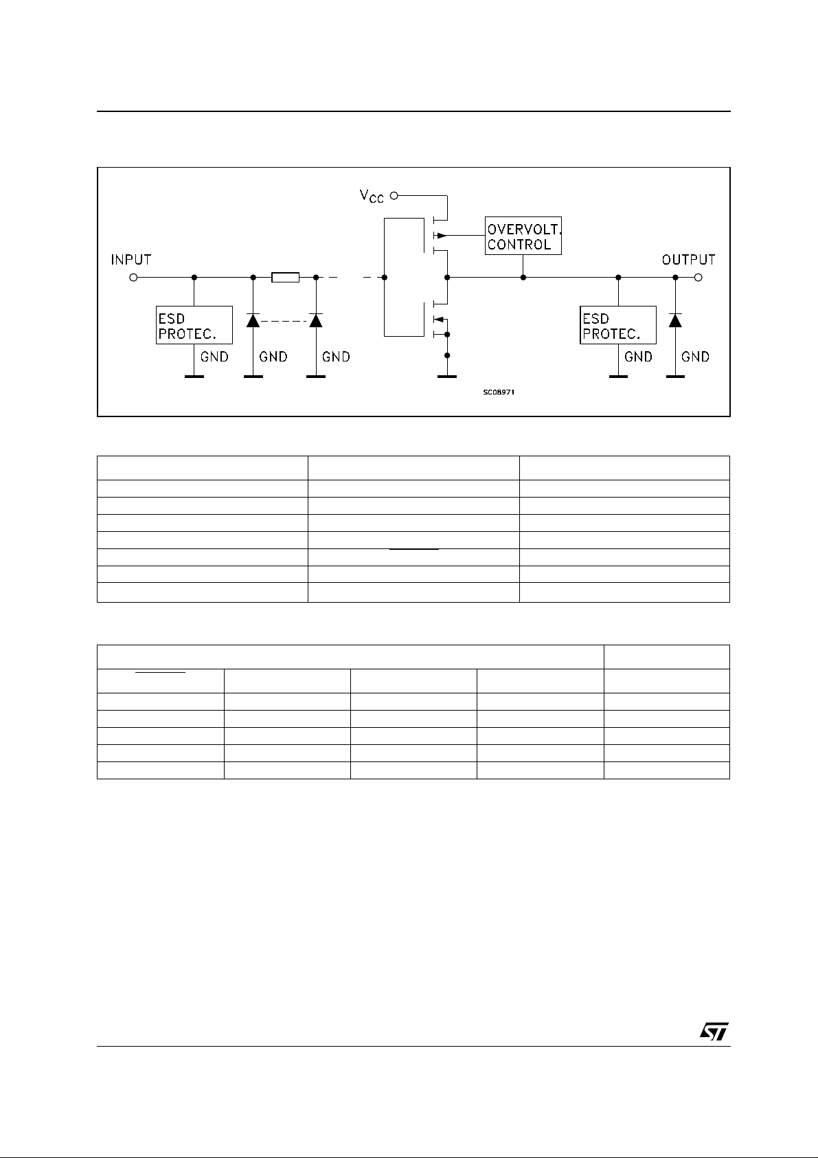
All inputs and outputs are equipped with
protection circuits against stat ic discharge, giving
them 2KV ESD immunity and transient excess
voltage.
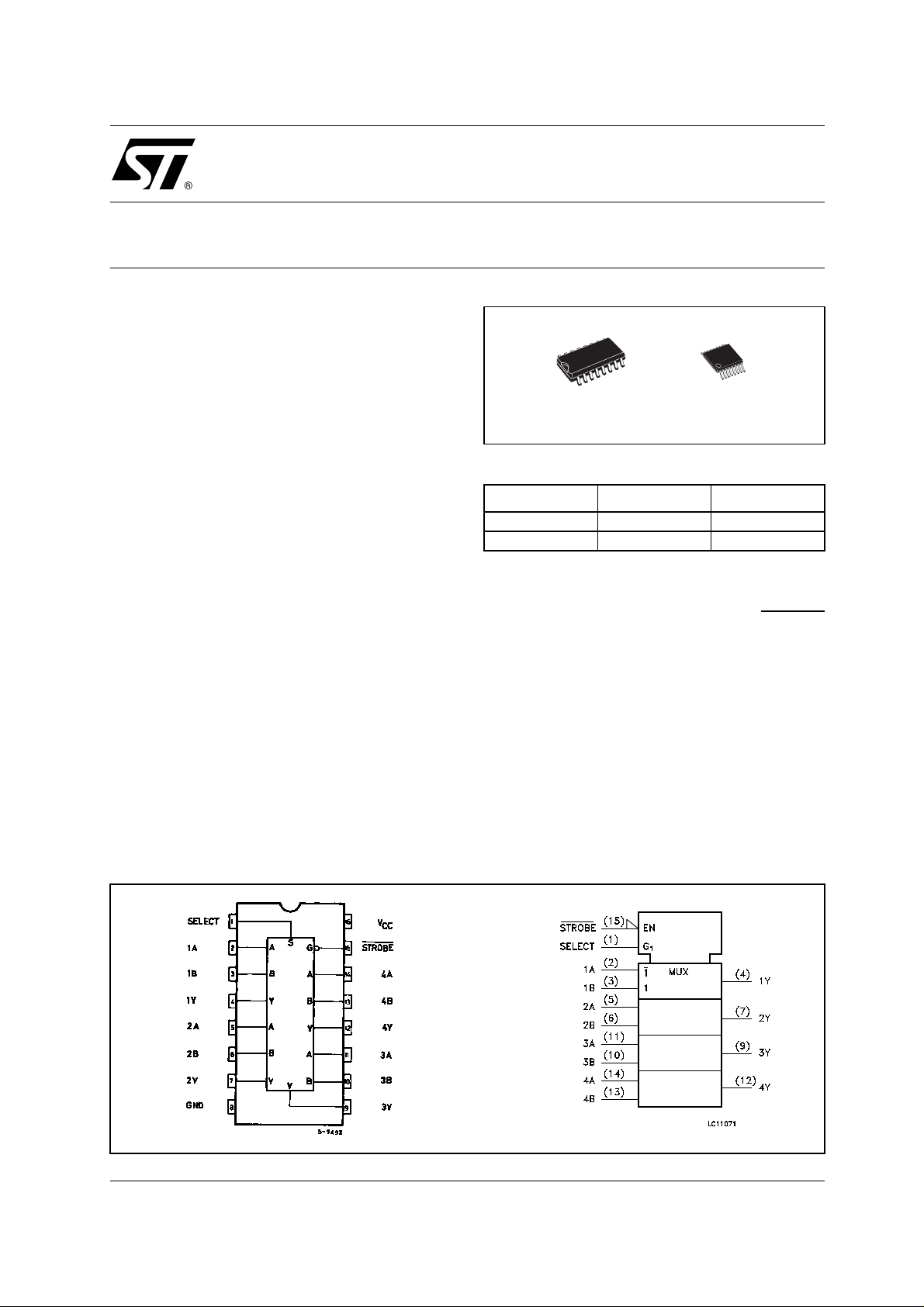
PIN CONNECTION AND IEC LOGIC SYMBOLS
1/9September 2001
74LCX157
INPUT AND OUTPUT EQUIVALENT CIRCUIT
PIN DESCRIPTION
PIN No SYMBOL NAME AND FUNCTION
1 SELECT Common Data Select Inputs
2, 5, 11, 14 1A to 4A Data Inputs From Source A
3, 6, 10, 13 1B to 4B Data Inputs From Source B
4, 7, 9, 12 1Y to 4Y Multiplexer Outputs
15 STROBE
8 GND Ground (0V)
16 V
CC
Strobe Input
Positive Supply Voltage
TRUTH TABLE
STROBE
HXXXL
LLLXL
LLHXH
LHXLL
LHXHH
X : Don’t Care
INPUTS OUTPUT
SELECT A B Y
2/9
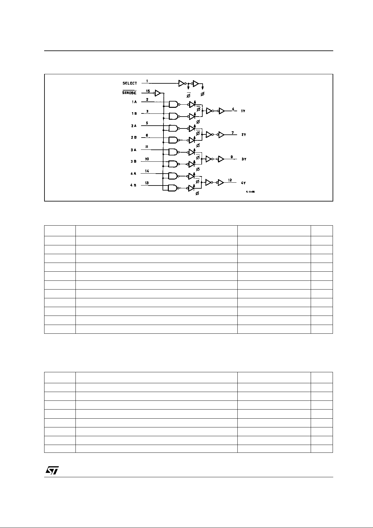
LOGIC DIAGRAM
This log i c diagram has not be used to esti m ate propaga tion delays
ABSOLUTE MAXIMUM RATINGS
74LCX157
Symbol Parameter Value Unit
V
V
V
V
I
I
OK
I
I
CC
I
GND
T
T
Absolute Maximum Ratings are those values beyond which damage to the device may occur. Functional operation under these conditions is
not implied
1) I
absolute ma xim um rating mu st be observed
O
2) V
< GND
O
Supply Voltage
CC
DC Input Voltage
I
DC Output Voltage (VCC = 0V)
O
DC Output Voltage (High or Low State) (note 1) -0.5 to VCC + 0.5
O
DC Input Diode Current
IK
DC Output Diode Current (note 2)
DC Output Current
O
DC Supply Current per Supply Pin
DC Ground Current per Supply Pin
Storage Temperature
stg
Lead Temperature (10 sec)
L
-0.5 to +7.0 V
-0.5 to +7.0 V
-0.5 to +7.0 V
V
- 50 mA
- 50 mA
± 50 mA
± 100 mA
± 100 mA
-65 to +150 °C
300 °C
RECOMMENDED OPERATING CONDITIONS
Symbol Parameter Value Unit
V
V
V
V
I
OH
I
OH
T
dt/dv Input Rise and Fall Time (note 2) 0 to 10 ns/V
1) Truth T abl e guaranteed: 1.5V to 3.6V
2) V
from 0.8V to 2V at VCC = 3.0V
IN
Supply Voltage (note 1)
CC
Input Voltage
I
Output Voltage (VCC = 0V)
O
Output Voltage (High or Low State) 0 to V
O
, I
High or Low Level Output Current (VCC = 3.0 to 3.6V)
OL
, I
High or Low Level Output Current (VCC = 2.7V)
OL
Operating Temperature
op
2.0 to 3.6 V
0 to 5.5 V
0 to 5.5 V
CC
± 24 mA
± 12 mA
-55 to 125 °C
V
3/9
 Loading...