

SGS Thomson Microelectronics 74GTL1655TTR Datasheet
1/14December 2001
■ HIGH SPEED GTL/GTL + UNIVER SAL
TRANSCEIVER :
t
PD
= 4.6 ns (MAX.) A to B at VCC = 3V
■ COMBINES D-TYPE L ATCHES AND D-T YPE
FLIP-FLOPS FOR OPERATION IN
TRANSPARENT, LATCHED, OR CLOCKED
MODE
■ OPERATING VOLTAGE RANGE:
V
CC
(OPR) = 3.0V to 3.6V
■ SYMMETRICAL OUTPUT IMPEDANCE:
|I
OH
| = IOL=24mA (MIN) at VCC = 3V (A PORT)
■ OUTPUT IMPEDANCE:
I
OL
= 100mA (MIN) at VCC = 3V (B PORT)
■ HIGH-IMPEDANCE ST ATE DURING POWER
UP AND POWER DOWN up to Vcc=1.5V
PERMITT LIVE INSERTION
■ B-PORT PRECHARGED BY BIASVcc
REDUCE NOISE ON THE LINE DURING
LIVE INSERTI O N
■ EDGE RATE-CONTROL INP U T
CONFIGURES THE B-PORT OUTPUT RISE
AND FALL TIMES
■ BUS HOLD ON DATA INPUTS ELIM INATES
THE NEED FOR EXTERNAL PULL-UP/
PULL-DOWN RESISTORS (A PO RT)
■ DISTRIBUTED VCC AND GND PIN
CONFIGURA TI ON MINIMIZES HIGH-SPEED
SWITCHING NOISE IN PARALLEL
COMUNICATIONS .
■ PIN AND FUNCTION COMPATIBLE WITH
74 SERIES 1655
DESCRIPTION
The 74GTL1655 devices are 16-bit high-drive
(100mA), low-output-impedance universal bus
transceivers designed for backplane applications.
The 74GTL1655 devices provide live-insertion
capability for backplane applications by tolerating
active signals on the data ports when the devices
are powered off. In addition, a biasing pin
preconditions the GTL/GTL+ port to minimize
disruption to an active backplane.
The edge rate-control (V
ERC
) input is provided so
the rise and fall time of the B outputs can be
configured to optimize for various backplane
loading conditions. Data flow in each direction is
controlled by output-enable (OEAB
and OEBA),
74GTL1655
16 BIT LVTTL TO GTL/GTL + UNIVERSAL BUS
TRANSCEIVERS WITH LIVE INSERTION
ORDER CODES
PACKAGE TUBE T & R
TSSOP 74GTL1655TTR
TSSOP
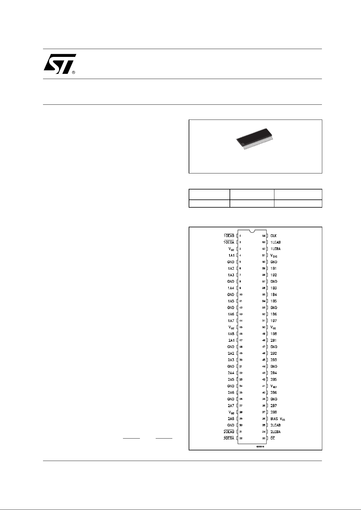
PIN CONNECTION

74GTL1655
2/14
latch-enable (LEAB and LEBA), and clock (CLK)
inputs. For A-to-B data flow, the devices operate
in the transparent mode when LEAB is high. When
LEAB is low, the A data is latched if CLK is held at
a high or lo w log ic level. If LEAB is low, the A data
is stored in the latch/flip-flop on the low-to-high
transition of CLK. When OEAB
is low, the outputs
are active. When OEAB
is high, the outputs are in
the high-impedanc e state. Data flow fo r B to A is
similar to that of A to B, but uses OEBA
, LEBA,
and CLK. The output enable (OE
) is used to
disable both ports simultaneously.
Active bus-hold circuitry is provided on the A port
to hold unu sed or floating data inputs at a valid
logic level. When V
CC
is between 0 and 1.5 V, the
device is in the high-impedance state during
power up or power down. Howe ve r, to en sure the
high-impedance st at e a bov e 1.5V , OE
should be
tied to V
CC
through a pullup resistor; the minimum
value of the resistor is determined by the
current-sinking capability of the driver.
All input and output are equipp ed with protection
circuits against static discharge, giving them 2KV
ESD immunity and transient excess voltage .
INPUT AND OUTPUT EQUIVALENT CIRCUIT
PIN DESCRIPTION
PIN N° SYMBOL NAME AND FUNCTION
1, 2 1OEAB
, 1OEBA Output Enable Input
4, 6, 7, 9, 11, 13, 14, 16 1A1 to 1A8 Data Inputs/Outputs LVTTL
17, 19, 20, 22, 23, 25, 27, 29 2A1 to 2A8 Data Inputs/Outputs LVTTL
31, 32 2OEAB
, 2OEBA Output Enable Input
33 OE
Output Enable Input
34, 35 2LEBA, 2LEAB Latch Enable
36 BIAS V
CC
Pre-Charge Supply Voltage
37, 38, 40, 42, 43, 45, 46, 48 2B8 to 2B1 Data Inputs/Outputs GTL/GTL+
41 V
REF
GTL Voltage Reference Input
49, 51, 52, 54, 55, 56, 58, 59 2A1 to 2A8 Data Inputs/Outputs GTL/GTL+
61 V
ERC
Edge Rate Control
62, 63 1LEBA, 1LEAB Latch Enable
64 CLK Clock Input (LOW to HIGH edge triggered)
5, 8, 10, 12, 18, 21, 24, 26, 30,
39, 44, 47, 53, 57, 60
GND Ground (0V)
3, 15, 28, 50 V
CC
Positive Supply Voltage
74GTL1655
3/14
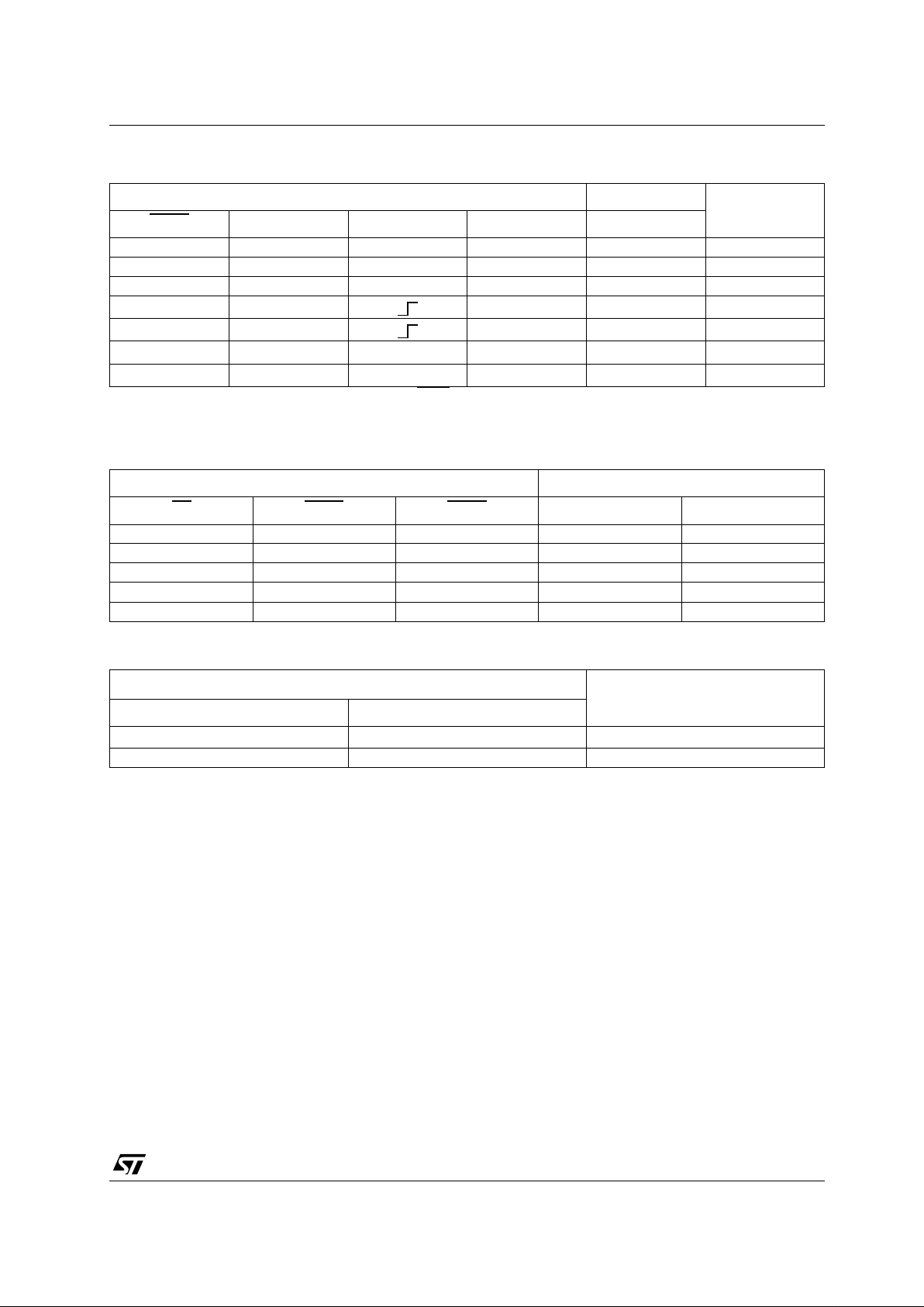
FUNCTION TABLE (1)
1) A to B data f l ow is shown. B to A flow is simi l ar, but uses OEBA , LEBA and CLK
2) Outp ut level before the indicated stead y-state inp ut conditions were est ablished, provided that CLK was high before LE AB went low
3) Output level before the indicated steady-state inp ut conditions were estab lis hed
OUTPUT ENABLE TRUTH TABLE
B-PORT EDGE RATE CONTROL (V
ERC
) TRUTH TABLE
INPUTS OUTPUT
MODE
OEAB
LEAB CLK A B
HXXXZIsolation
L H X L L Transparent
L H X H H Transparent
L L L L Registered
L L H H Registered
LLHX
B0
(2)
Previous State
LLLX
B0
(3)
Previous State
INPUTS OUTPUTS
OE
OEAB OEBA A PORT B PORT
L L L Active Active
L L H Z Active
L H L Active Z
LHHZZ
HXXZZ
INPUT V
ERC
OUTPUT B PORT EDGE RATE
LOGIC LEVEL NOMINAL VOLTAGE
H
V
CC
Slow
L GND Fast
74GTL1655
4/14
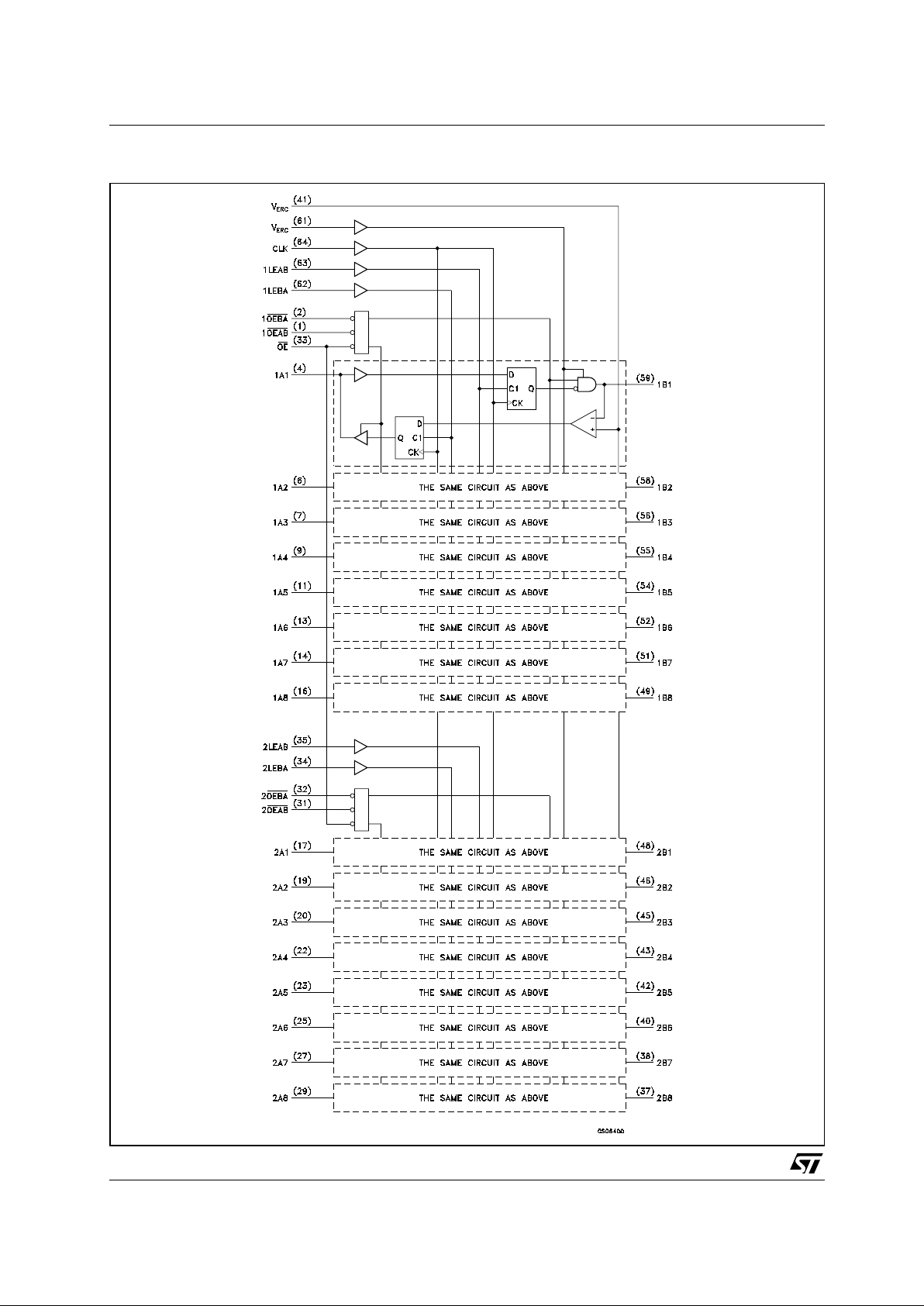
LOGIC DIAGRAM

74GTL1655
5/14
ABSOLUTE MAXIMUM RATINGS
Absolute Maximum Rating are those value beyond which damage to the device may occur. Functional operation under these condition is not
implied
RECOMMENDED OPERATING CONDITIONS
1) VTT and RTT can be adjus ted to adapt backplane impedance if DC raccomanded IOL ratings are not exceed ed
2) V
REF
can be adjusted to optimaze noise margin (typ two-thirds VTT)
Symbol Parameter Value Unit
V
CC
Supply Voltage, Bias V
CC
-0.5 to +4.6 V
V
IA
DC Input Voltage A Side, Control Input
-0.5 to +4.6 V
V
IB
DC Input Voltage B Side, V
ERC
, V
REF
-0.5 to +4.6 V
V
OA
DC Output Voltage A Side
-0.5 to +4.6 V
V
OB
DC Output Voltage B Side
-0.5 to +4.6 V
I
IK
DC Input Diode Current
- 50 mA
I
OK
DC Output Diode Current
- 50 mA
I
OA
DC Output Current A Side
± 48 mA
I
OB
DC Output Current B Side in the Low State
200 mA
T
stg
Storage Temperature
-65 to +150 °C
T
L
Lead Temperature (10 sec)
300 °C
Symbol Parameter
Value
Unit
Min. Typ. Max.
V
CC
Supply Voltage
3.0 3.3 3.6 V
V
TT
Termination Voltage GTL 1.14 1.2 1.26
V
GTL+ 1.35 1.5 1.65
V
REF
Supply Voltage GTL 0.74 0.8 0.87
V
GTL+ 0.87 1 1.1
V
I
Input Voltage B port
0
V
TT
V
other
0
V
CC
V
IH
High Level Input Voltage B port V
REF
+0.05
V
other 2
V
IL
Low Level Input Voltage B port V
REF
-0.05
V
other 0.8
I
IK
Input Clamp Current
-18 mA
I
OH
High Level Output Current A port
-24 mA
I
OL
Low Level Output Current A port 24
mA
B port 100
dt/dV
CC
Power -up ramp rate
200 µs/V
T
op
Operating Temperature
-40 85 °C
 Loading...