

SGS Thomson Microelectronics 74ALVCH162373T Datasheet
74ALVCH162374
LOW VOLTAGE CMOS 16-BIT D-TYPE FLIP-FLOP (3-STATE)
WITH 3.6V TOLERANT INPUTS AND OUTPUTS
PRELIMINARY DATA
■ 3.6V TOLERANT INPUTS AND OUTPUTS
■ HIGH SPEED :
= 4.6 ns (MAX.) at VCC=3.0to3.6V
t
PD
t
= 5.4 ns (MAX.) at VCC=2.3to2.7V
PD
t
= 6.5 ns (MAX.) at VCC=1.65V
PD
■ POWER DOWN PROTECTION ON INPUTS
AND OUTPUTS
■ SYMMETRICAL OUTPUT IMPEDANCE:
|=IOL= 24mA (MIN) at VCC=3.0V
|I
OH
|I
|=IOL= 18mA (MIN) at VCC=2.3V
OH
|I
|=IOL=4mA(MIN)atVCC= 1.65V
OH
■ BUS HOLD PROVIDED ON DATA INPUTS
■ 26Ω SERIE RESISTORS IN OUTPUTS
■ OPERATING VOLTAGE RANGE:
(OPR) = 1.65V to 3.6V
V
CC
■ PIN AND FUNCTION COMPATIBLE WITH
74 SERIES 16374
■ LATCH-UP PERFORMANCE EXCEEDS
300mA (JESD 17)
■ ESD PERFORMANCE:
HBM > 2000V (MIL STD 883 method 3015);
MM > 200V
ORDER CODES
PACKAGE TUBE T & R
TSSOP 74ALVCH162374TTR
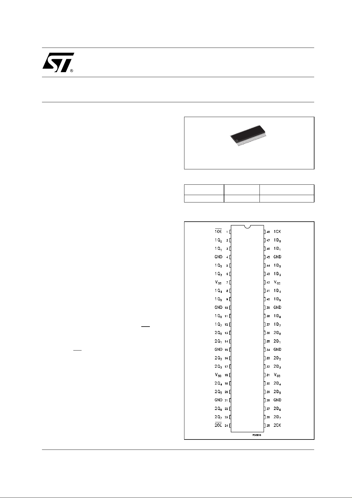
PIN CO NNE CTION
TSSOP
DESCRIPTION
The 74ALVCH162374 is a low voltage CMOS 16
BIT D-TYPE LATCH with 3 STATE OUTPUTS
NON INVERTING fabricated with sub-micron
silicon gate and five-layer metal wiring C
2
MOS
technology. It is ideal for low power and very high
speed 1.65 to 3.6V applications; it can be
interfaced to 3.6V signal environment for both
inputs and outputs.
These flip-flops are controlled by two clock inputs
(nCK) and two output enable inputs (nOE
).
Onthepositivetransitionofthe(nCK),thenQ
outputs wi ll be set to the logic state that were
setup at the nD inputs.
While the (nOE
) in put is low, the outputs (nQ) will
be in a normal state (HIGH or LOW logic level)
and while high level the out puts will be in a hi gh
impedance state.
Any output control does not af fect the interna l
operation of flip flops; that is, the old data can be
retained or the new data can be entered even
while the out put s are off.The device circuits is
including 26Ω series resistance in the out puts.
These resistors permit to reduc e line noise in high
speed applications.
All inputs and outputs are equipped with
protection circuits against stat ic discharge, giving
them 2KV ESD immunity and transient excess
voltage.
1/11February 2003
This is preliminary information on a new product now in development are or undergoing evaluation. Details subject to change without notice.
74ALVCH162374
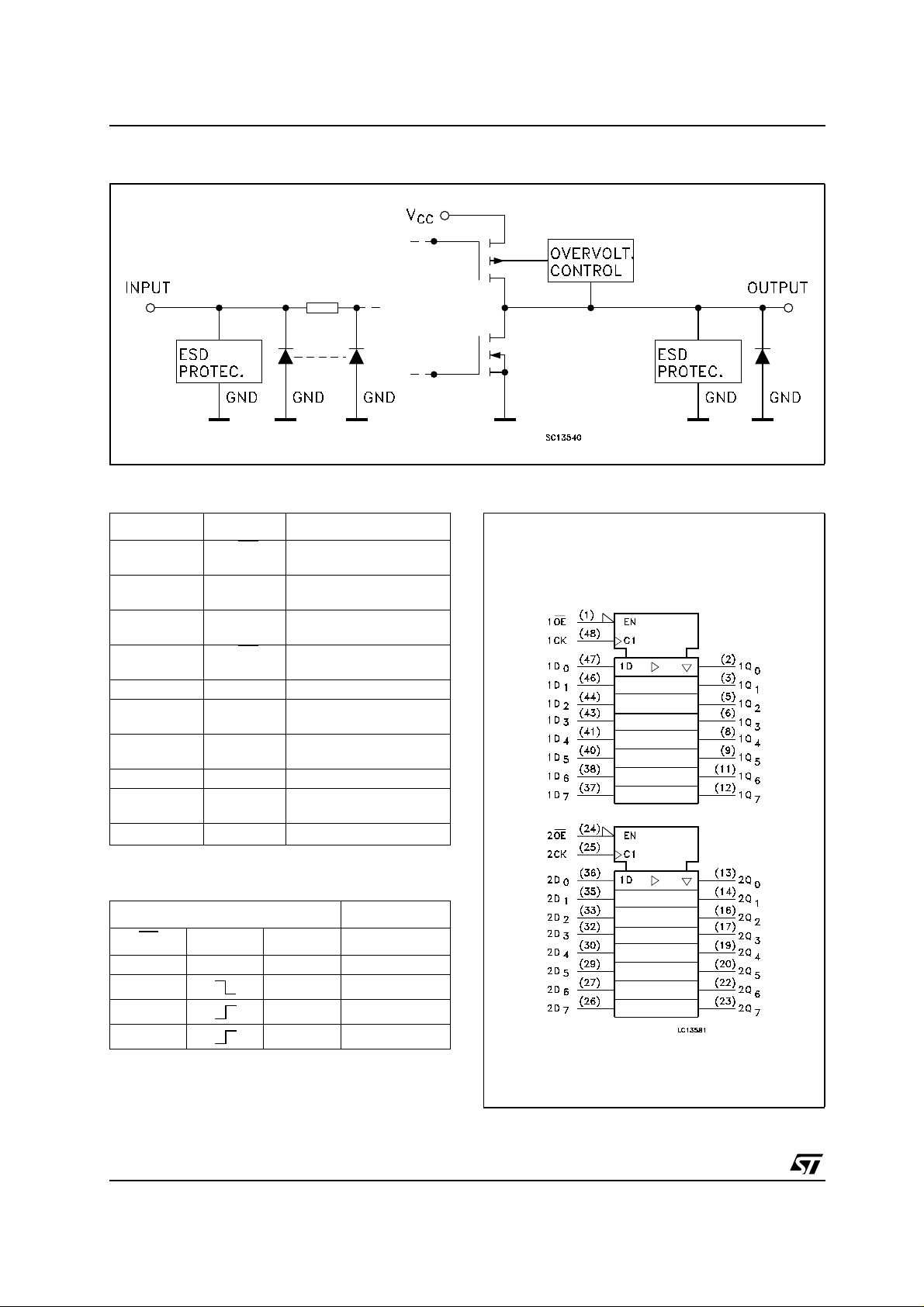
INPUT AND OUTPUT EQUIVALENT CIRCUIT
PIN DESCRIPTION
PIN No SYMBOL NAME AND FUNCTION
1 1OE
2, 3,5,6,8,9,
11, 12
13,14,16,17,
19, 20, 22, 23
24 2OE
25 2CK Clock Input
36,35,33,32,
30, 29, 27, 26
47,46,44,43,
41, 40, 38, 37
48 1CK Clock Input
4, 10, 15, 21,
28, 34, 39, 45
7, 18, 31, 42 V
1Q0 to 1Q7 3-State Outputs
2Q0 to 2Q7 3-State Outputs
2D0 to 2D7 Data Inputs
1D0 to 1D7 Data Inputs
GND Ground (0V)
CC
3 State Output Enable
Input (Active LOW)
3 State Output Enable
Input (Active LOW)
Positive Supply Voltage
TRUTH TABLE
INPUTS OUTPUT
OE
HXX Z
L X NO CHANGE
LLL
LHH
CK D Q
IEC LOGIC SYMBOLS
X : Don‘t Care
Z : High Impedance
2/11
74ALVCH162374
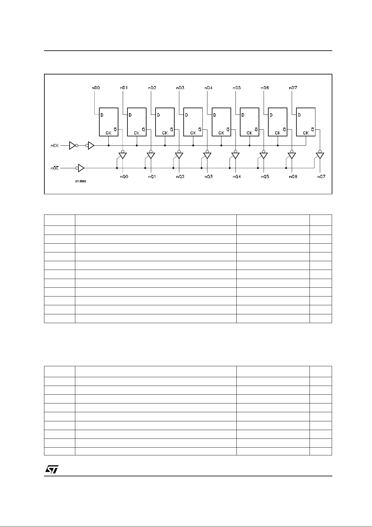
LOGIC DIAGRAM
ABSOLUTE MAXIMUM RATINGS
Symbol Parameter Value Unit
V
CC
V
V
V
I
IK
I
OK
I
or I
I
CC
P
T
stg
T
Absolute Maximum Ratings are those values beyond which damage to the device may occur. Functional operation under these conditions is
not implied
absolute maximum rating must be observed
1) I
O
2) V
<GND,VO>V
O
Supply Voltage
DC Input Voltage
I
DC Output Voltage (OFF State)
O
DC Output Voltage (High or Low State) (note 1) -0.5 to VCC+ 0.5
O
DC Input Diode Current
DC Output Diode Current (note 2)
DC Output Current
O
DC VCCor Ground Current per Supply Pin
GND
Power Dissipation
D
Storage Temperature
Lead Temperature (10 sec)
L
CC
-0.5 to +4.6 V
-0.5 to +4.6 V
-0.5 to +4.6 V
V
-50 mA
-50 mA
± 50 mA
± 100 mA
400 mW
-65 to +150 °C
300 °C
RECOMMENDED OPERATING CONDITIONS
Symbol Parameter Value Unit
V
CC
V
V
V
I
OH,IOL
I
OH,IOL
I
OH,IOL
T
dt/dv Input Rise and Fall Time (note 1) 0 to 10 ns/V
1) VINfrom0.8V to 2Vat VCC=3.0V
Supply Voltage
Input Voltage
I
Output Voltage (OFF State)
O
Output Voltage (High or Low State) 0 to V
O
High or Low Level Output Current (VCC= 3.0 to 3.6V)
High or Low Level Output Current (VCC= 2.3 to 2.7V)
High or Low Level Output Current (VCC= 1.65V)
Operating Temperature
op
1.65 to 3.6 V
-0.3 to 3.6 V
0 to 3.6 V
CC
± 12 mA
± 6mA
± 2mA
-55 to 125 °C
V
3/11
74ALVCH162374
DC SPECIFICATIONS
Test Condition Value
Symbol Parameter
V
V
V
I
IHOLD
High Level Input
IH
Voltage
V
Low Level Input
IL
Voltage
High Level Output
OH
Voltage
Low Level Output
OL
Voltage
Input Leakage
I
I
Current
Bus Hold Input
Leakage Current
Power Off Leakage
I
off
Current
I
High Impedance
OZ
Output Leakage
Current
I
∆I
Quiescent Supply
CC
Current
CCICC
incr. per Input 3.0 to 3.6 VIH=VCC- 0.6V 500 750 µA
V
CC
(V)
-40 to 85 °C -55 to 125 °C
Min. Max. Min. Max.
1.65 to 1.95 0.65 Vcc 0.65 Vcc
2.3 to 2.7 1.7 1.7
2.7 to 3.6 2.0 2.0
1.65 to 1.95 0.35 Vcc 0.35 Vcc
2.3 to 2.7 0.7 0.7
2.7 to 3.6 0.8 0.8
1.65 to 3.6
1.65
2.3
2.3
2.7
3.0
3.0
1.65 to 3.6
1.65
2.3
2.3
2.7
3.0
3.6
1.65
1.65
2.3
2.3
3.0
3.0
3.6
0V
3.6 V
3.6 VI=VCCor GND
IO=-100 µAVCC-0.2 VCC-0.2
I
=-2 mA
O
=-4 mA
I
O
=-6 mA
I
O
=-8 mA
I
O
=-6 mA
I
O
=-12 mA
I
O
=100 µA
I
O
=2 mA
I
O
=4 mA
I
O
=6 mA
I
O
=8 mA
I
O
=12 mA
I
O
= 0 or 3.6V
V
I
VI=0.58 V
=1.07 V
V
I
=0.7 V
V
I
=1.7 V
V
I
=0.8 V
V
I
=2 V
V
I
= 0 to 3.6 V
V
I
or VO= 3.6V 10 20 µA
I
or V
I=VIH
VO= 0 to V
IL
CC
1.2 1.2
2.0 2.0
1.7 1.7
2.2 2.2
2.4 2.4
2.0 2.0
0.2 0.2 V
0.45 0.45
0.4 0.4
0.55 0.55
0.6 0.6
0.8 0.8
± 5 ± 5 µA
+25 +25
-25 -25
+45 +45
-45 -45
+75 +75
-75 -75
± 500 ± 500
± 5 ± 10 µA
20 40 µA
I
=0
O
Unit
V
V
µA
4/11
 Loading...