

■ OPERATES4 LATCHINGRELAIS, 1SINGLE
SIDESTABLERELAYAND1 LED
■ VERYLOWPOWERCONSUMPTION
■
TTL COMPATIBLEINPUT THRESHOLDS
■ IMPROVEDLATCH-UP IMMUNITY UPTO
300mA
■
TSSOP-20PACK AGE
DESCRIPTION
The device is a relais driver for line card
application. It is able to operate four latching
relais, one single side stable relay and one LED
connected either to GND or VCC. All the outputs
can be set to LOW with the RST input as shown
in thetrue table.
74ACT8244
RELAY DRIVER IC
T
(TSSOPPackage)
ORDERCODES :
74ACT8244TTR
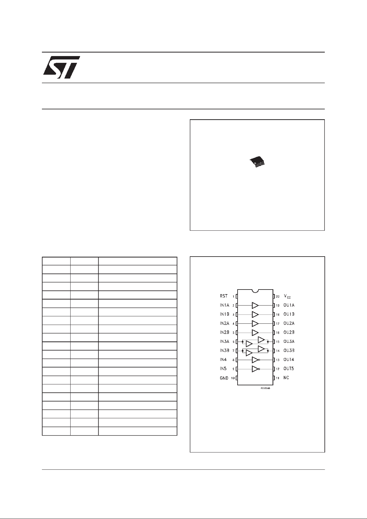
PIN DESCRIPTION
PI N No SYMB O L NAM E AND F UNCT ION
1 RST Master Reset
2 IN1A Input of 1st latched relay drv
3 IN1B Input of 1st latched relay drv
4 IN2A Input of 2nd latched relay drv
5 IN2B Input of 2nd latched relay drv
6 IN3A Input of 3rd latched relay drv
7 IN3B Input of 3rd latched relay drv
8 IN4 Input of 1st relay driver
9 IN5 Input LED driver
10 GND Ground
11 NC Not Connected
12 OUT5 Output of LED driver
13 OUT4 Output of 1st relay driver
14 OU3B Output 3rd latched relay drv
15 OU3A Output 3rd latched relay drv
16 OU2B Output 2nd latched relay drv
17 OU2A Output 2nd latched relay drv
18 OU1B Output 1st latched relay drv
19 OU1A Output 1st latched relay drv
20 V
CC
Supply Voltage
LOGICDIAGRAM
November 1999
1/6

74ACT8244
ABSOLUTE MAXIMUMRATINGS
Symb o l Para met er Val u e Uni t
V
V
V
I
I
OK
I
orI
I
CC
T
AbsoluteMaximumRatingsarethosevaluesbeyond whichdamagetothedevicemayoccur. Functionaloperationunderthesecondition isnotimplied.
RECOMMENDEDOPERATINGCONDITIONS
Symb o l Parameter Val u e Uni t
V
V
V
T
dt/dv Input Rise and Fall Time V
1)VINfrom0.8V to2.0V
Supply Voltage -0.5to+7 V
CC
DC Input Voltage -0.5toVCC+0.5 V
I
DC Output Voltage -0.5toVCC+0.5 V
O
DC Input Diode Current ±50 mA
IK
DC Output Diode Current ±50 mA
DC Output Current
O
DC VCCor Ground Current
GND
Storage Temperature -65to+150
stg
Supply Voltage 4.75to5.25 V
CC
Input Voltage 0toV
I
Output Voltage 0toV
O
Operating Temperature: -30to+80
op
= 4.5 to 5.5V (note1) 10 ns/V
CC
100 mA
±
400 mA
±
CC
CC
o
C
V
V
o
C
DC SPECIFICATIONS (Electricalcharacteristics over recommendedoperating conditions)
Symb o l Parame t er Test Cond ition s Value Unit
Min. T yp. Max.
High Level Input Threshold VO=0.1V or VCC- 0.1 V 2.0 1.4 V
V
IH
Low Level Input Threshold VO=0.1V or VCC- 0.1 V 1.4 0.8
V
IL
High Level Output Voltage for
V
OH
Single Driver
Low Level Output Voltage for
V
OL
Single Driver
High Level Output Voltage for
V
OH
Double Relay Driver
Low Level Output Voltage for
V
OL
Double Relay Driver
High Level Output Voltage for
V
OH
Single Side Relay or LED
Low Level Output Voltage for
V
OL
Single Side Relay or LED
Input Leakage Current VI=VCCor GND ±1 µA
I
I
Max ICC/Input VI=VCC-2.1V 0.6 1.5 mA
I
CCT
Quiescent Supply Current VI=VCCor GND 4 40 µA
I
CC
I
=-35mA VCC-0.68 VCC-0.3 V
OUT
I
= 35mA 0.25 0.68 V
OUT
I
=-70mA VCC-0.68 VCC-0.3 V
OUT
I
= 70mA 0.25 0.68 V
OUT
I
=-50mA VCC-0.8 VCC-0.4 V
OUT
I
=50mA 0.3 0.8 V
OUT
V
2/6
 Loading...