

SGS Thomson Microelectronics 74ACT373 Datasheet
74ACT373
OCTAL D-TYPE LATCH
WITH 3 STATE OUTPUT NON INVERTING
■ HIGH SPEED: t
■ LOWPOWERDISSIPATION:
=8µA (MAX.)at TA=25oC
I
CC
■ COMPATIBLEWITH TTL OUTPUTS
V
=2V(MIN),VIL= 0.8V (MAX)
IH
■ 50Ω TRANSMISSIONLINE DRIVING
=6 ns (TYP.)atVCC=5V
PD
CAPABILITY
■ SYMMETRICAL OUTPUT IMPEDANCE:
|I
|=IOL=24mA(MIN)
OH
■ BALANCED PROPAGATIONDELAYS:
t
≅ t
PLH
PHL
■ OPERATINGVOLTAGERANGE:
V
(OPR)= 4.5V to 5.5V
CC
■ PIN AND FUNCTION COMPATIBLE WITH
74SERIES373
■ IMPROVED LATCH-UP IMMUNITY
DESCRIPTION
The ACT373 is an advanced high-speed CMOS
OCTAL D-TYPE LATCH with 3 STATE OUTPUT
NON INVERTING fabricated with sub-micron
silicon gate and double-layermetal wiring C
2
MOS
technology. It is ideal for low power applications
mantaining high speed operation similar to
equivalentBipolar Schottky TTL.
These 8 bit D-Type latch are controlledby a latch
enable input (LE) and an output enable input
B
(Plastic Package)
(Micro Package)
M
ORDER CODES :
74ACT373B 74ACT373M
(OE).
While the LE inputs is held at a high level, the Q
outputs will follow the data input precisely or
inversely. When the LE is taken low, the Q
outputs will be latched precisely or inversely at
the logic level of D input data. While the (OE)
input is low, the 8 outputs will be in a normallogic
state (high or low logic level) and while high level
the outputs will be in a high impedance state.
This device is designed to interface directly High
Speed CMOS systems with TTL and NMOS
components.
All inputs and outputs are equipped with
protectioncircuits against static discharge, giving
them 2KV ESD immunity and transient excess
voltage.
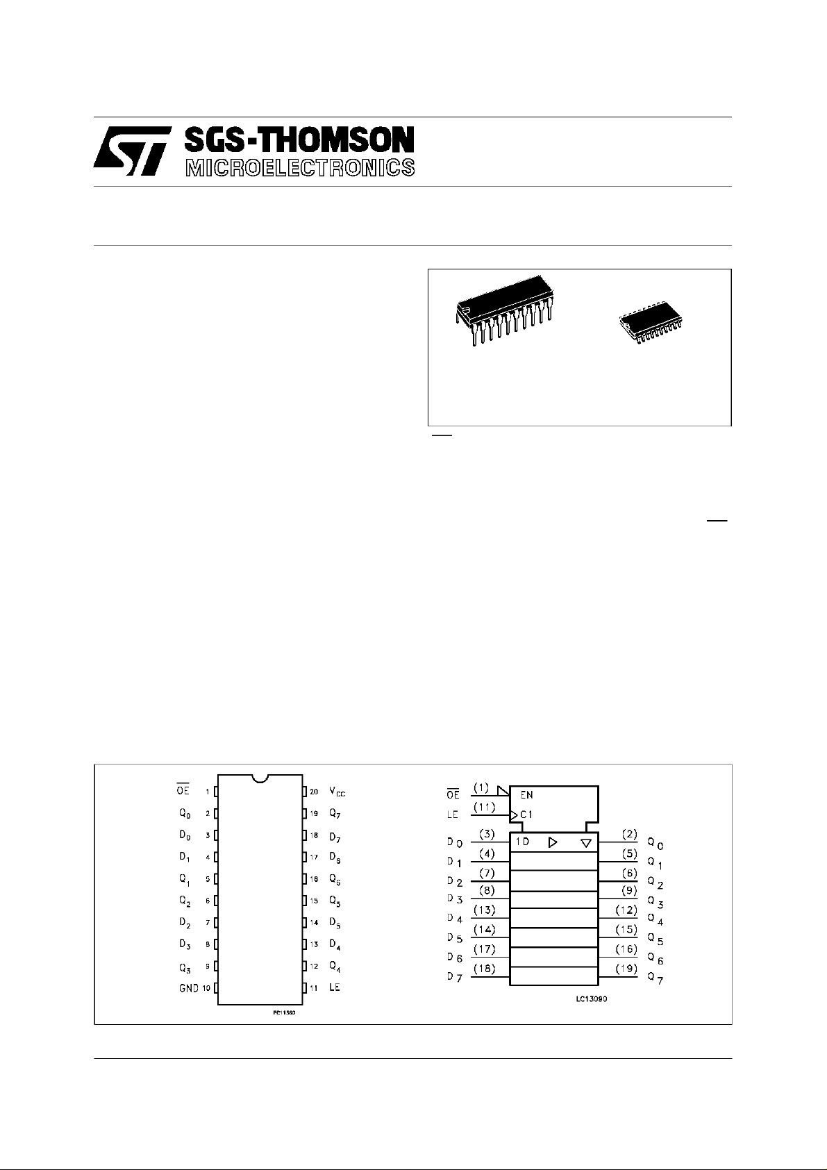
PINCONNECTION AND IEC LOGIC SYMBOLS
April 1997
1/10
74ACT373
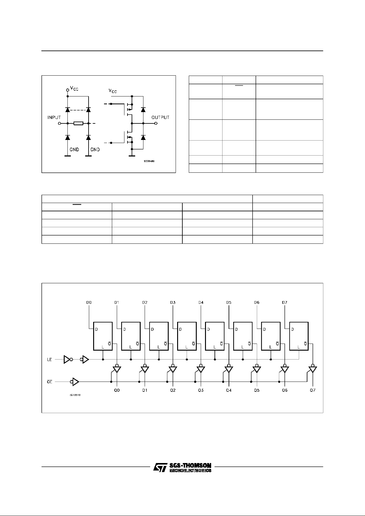
INPUTAND OUTPUTEQUIVALENTCIRCUIT PIN DESCRIPTION
PI N No SYM B O L NAME AN D FUNCT I ON
1 OE 3 State Output Enable
2, 5, 6,
9, 12, 15,
16, 19
3, 4, 7,
8, 13, 14,
17, 18
11 LE Latch Enable
10 GND Ground (0V)
20 V
TRUTH TABLE
INPUTS OUTPUTS
OE LE D Q
HXXZ
L L X NO CHANGE *
LHLL
LHHH
X:DON’T CARE
Z:HIGHIMPEDANCE
*:Q OUTPUTS ARE LATCHED AT THE TIMEWHENTHE LE INPUTIS TAKEN LOWLOGIC LEVEL.
Q0 to Q7 Data Inputs
D0 to D7 3 State Outputs
CC
Input (Active LOW)
Input
Positive Supply Voltage
LOGICDIAGRAMS
2/10
74ACT373
ABSOLUTE MAXIMUM RATINGS
Symb o l Parameter Val u e Uni t
V
V
V
I
I
OK
I
orI
I
CC
T
T
Absolute Maximum Ratings are those values beyond which damage to the device may occur. Functional operation under these condition is not implied.
RECOMMENDEDOPERATINGCONDITIONS
Symbol Parameter Valu e Unit
V
V
V
T
dt/dv Input Rise and Fall Time V
1) VINfrom0.8Vto2.0V
Supply Voltage -0.5 to +7 V
CC
DC Input Voltage -0.5 to VCC+ 0.5 V
I
DC Output Voltage -0.5 to VCC+ 0.5 V
O
DC Input Diode Current ± 20 mA
IK
DC Output Diode Current ± 20 mA
DC Output Current ± 50 mA
O
DC VCCor Ground Current ± 400 mA
GND
Storage Temperature -65 to +150
stg
Lead Temperature (10 sec) 300
L
Supply Voltage 4.5 to 5.5 V
CC
Input Voltage 0 to V
I
Output Voltage 0 to V
O
Operating Temperature: -40 to +85
op
= 4.5 to 5.5V (note 1) 8 ns/V
CC
CC
CC
o
C
o
C
V
V
o
C
3/10
 Loading...