WITH ASYNCHRONOUS CLEAR
■ HIGHSPEED:
=170MHz(TYP.)at VCC=5V
f
MAX
■ LOWPOWER DISSIPATION:
=8 µA (MAX.) at TA=25oC
I
CC
■ COMPATIBLEWITHTTL OUTPUTS
=2V(MIN),VIL=0.8V(MAX)
V
IH
■ 50Ω TRANSMISSIONLINEDRIVING
CAPABILITY
■ SYMMETRICALOUTPUTIMPEDANCE:
|=IOL=24mA(MIN)
|I
OH
■ BALANCEDPROPAGATIONDELAYS:
≅ t
t
PLH
PHL
■ OPERATINGVOLTAGERANGE:
(OPR)= 4.5Vto 5.5V
V
CC
■ PINANDFUNCTIONCOMPATIBLEWITH
74SERIES299
■ IMPROVEDLATCH-UP IMMUNITY
DESCRIPTION
The ACT299 is an high-speedCMOS 8-BIT PIPO
SHIFT REGISTERS (3-STATE) fabricated with
sub-micron silicon gate and double-layer metal
wiring C
power applications mantaining high speed
operation similar to equivalent Bipolar Schottky
TTL.
2
MOS technology. It is ideal for low
74ACT299
8 BIT PIPO SHIFT REGISTER
PRELIMINARY DATA
B
(PlasticPackage)
(Micro Package)
ORDERCODES :
74ACT299B 74ACT299M
These devices have four modes (HOLD, SHIFT
LEFT, SHIFT RIGHT and LOAD DATA). Each
mode is chosenby two functionselect inputs (S0,
S1)as shownin the TruthTable.
When one or both enable inputs, (G1, G2) are
high, the eight input/output terminals are in
the high-impedance state ; however sequential
operation or clearing of the register is not
affected.Clear function is synchronousto clock.
The device is designed to interface directly High
Speed CMOS systems with TTL, NMOS and
CMOSoutput voltage levels.
All inputs and outputs are equipped with
protection circuits against static discharge, giving
them 2KV ESD immunity and transient excess
voltage.
M
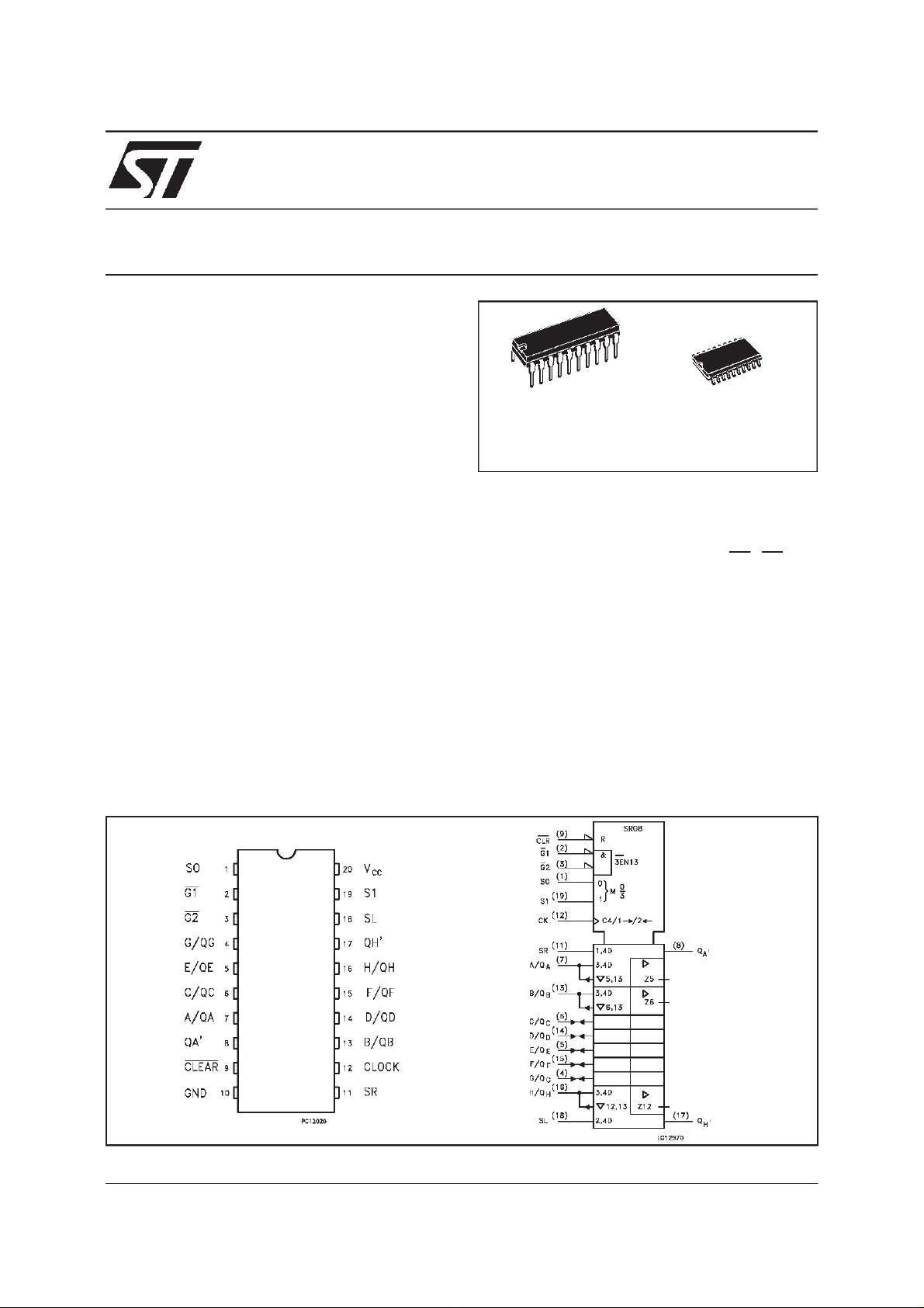
PIN CONNECTIONAND IEC LOGIC SYMBOLS
April 1999
1/13

74ACT299
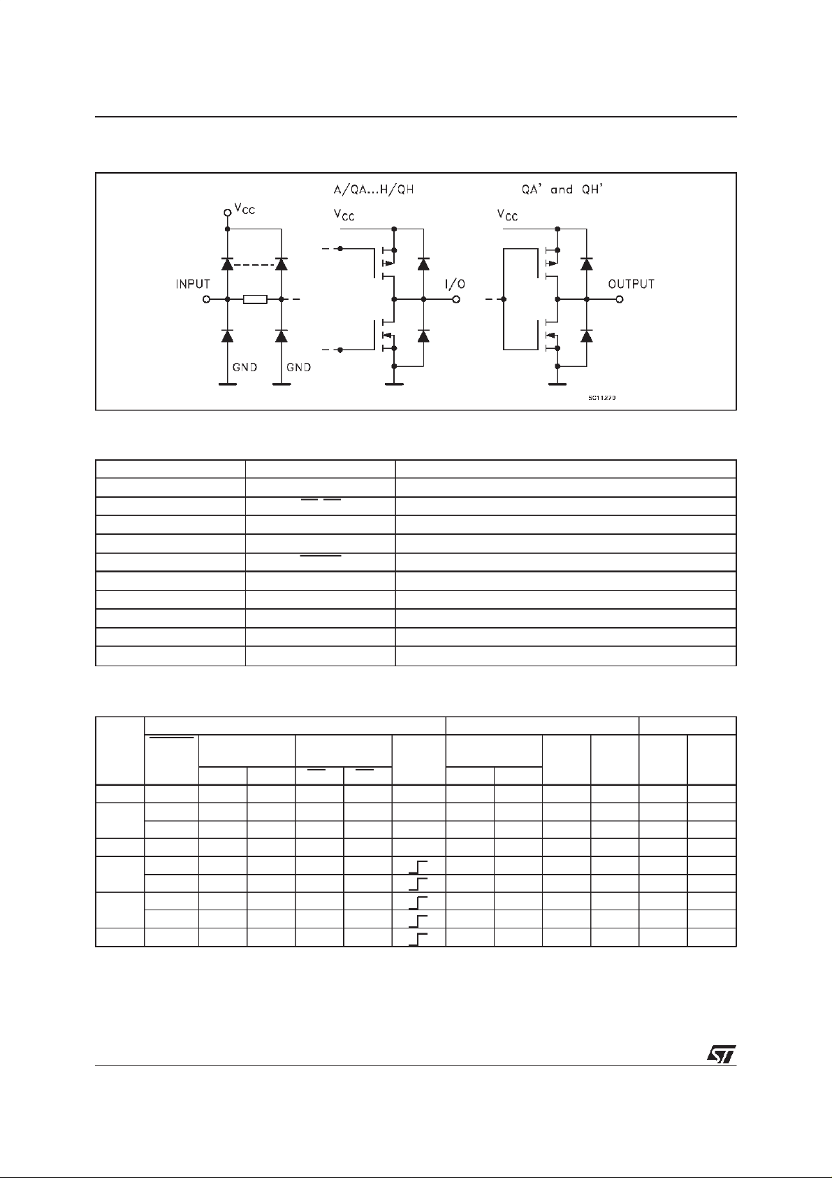
INPUT AND OUTPUT EQUIVALENT CIRCUIT
PIN DESCRIPTION
PIN No SYM BO L NAME AND FUNCT I O N
1, 19 S0, S1 Mode Select Inputs
2, 3 G1, G2 3 State Output Enable Inputs (Active LOW)
7, 13, 6,14, 5, 15, 4, 16 A/QA to H/QH Parallel Data Inputs or 3 State Parallel Outputs (Bus Driver)
8, 17 QA’ to QH’ Serial Outputs (Standard Output)
9 CLEAR Asynchronous Master Reset Input (Active LOW)
11 SR Serial Data Shift Right Input
12 CLOCK Clock Input (LOW to HIGH, Edge-triggered)
18 SL Serial Data Shift Left Input
10 GND Ground (0V)
20 V
CC
Positive Supply Voltage
TRUTH TABLE
MODE INPUTS INPUT S/ OUTPU TS O UT PUT S
CLEAR
FUNCTION
SELECTED
S1 S0 G1* G2* SL SR
Z L HHXX X XXZZL L
CLEAR L L X L L X X X LLLL
LXLLLXXXLLLL
HOLD H LLLLXXXQA0QH0QA0QH0
SHIFT
RIGHT
SHIFT
LEFT
H L H L L X H H QGn H QGn
H L H L L X L L QGn L QGn
H H L L L H X QBn H QBn H
H H L L L L X QBn L QBn L
LOAD H H H X X X X ahah
* Whenone or bothoutputcontrols arehigh, theeight, input/output terminals are thehigh impedanc e state:howewer sequential operationor clearing of
theregister isnotaffected.
Z :HIGHIMPEDANCE
Qn0 : THELEVELOF AnBEFORETHEINDICATEDSTEADYSTATEINPUTCONDITIONS WEREESTABLISED.
Qnn :THELEVELOF QnBEFORETHE MOSTRECENTACTIVETRANSITIONINDICATEDBYOR
a,h :THELEVELOFTHESTEADYSTATEINPUTSA,H,RESPECTIVELY.
X :DON’TCARE
2/13
OUTPUT
CONTROL
CLOCK SERIAL A/QA H/QH QA’ QH’

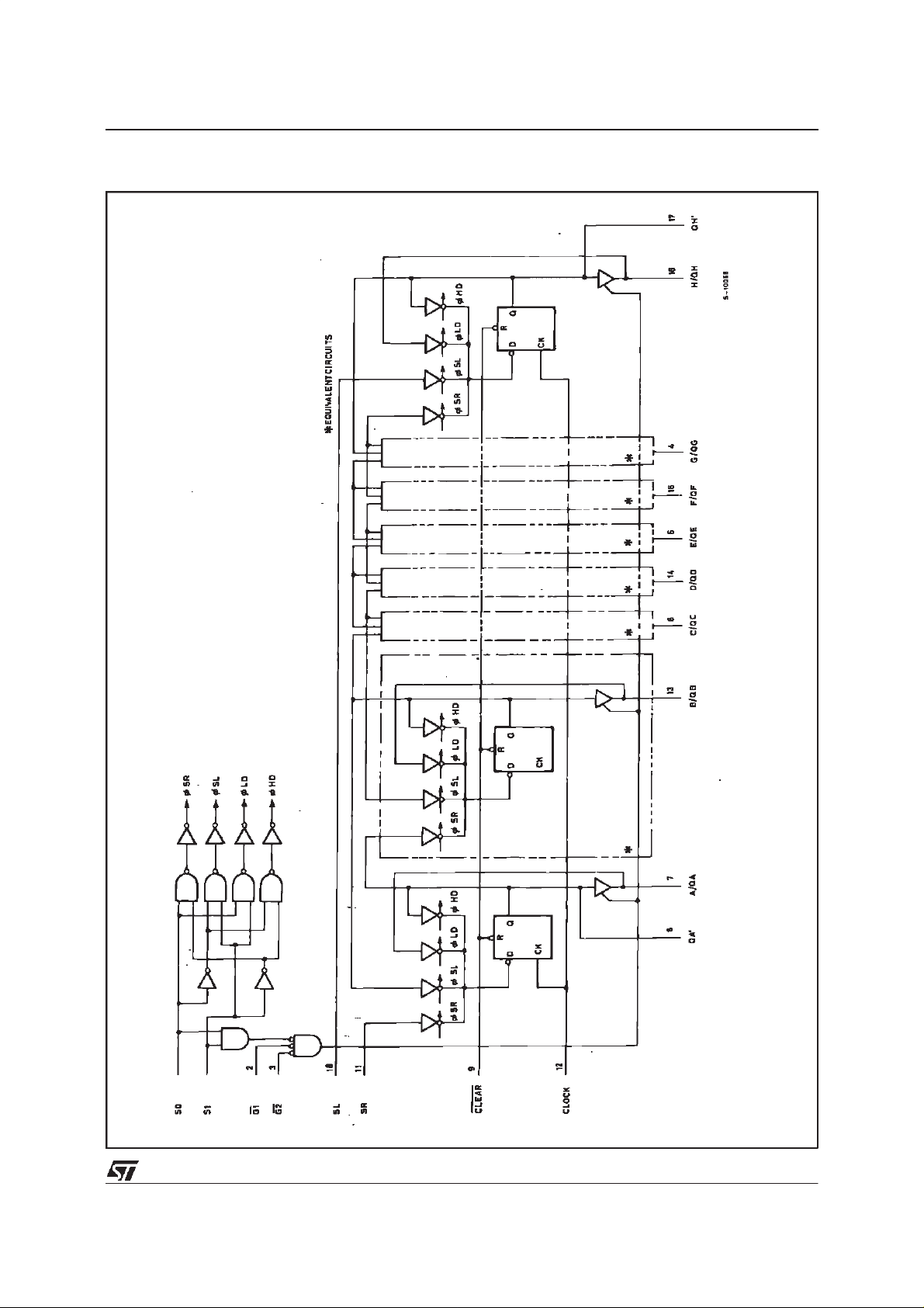
LOGICDIAGRAM
74ACT299
3/13

74ACT299
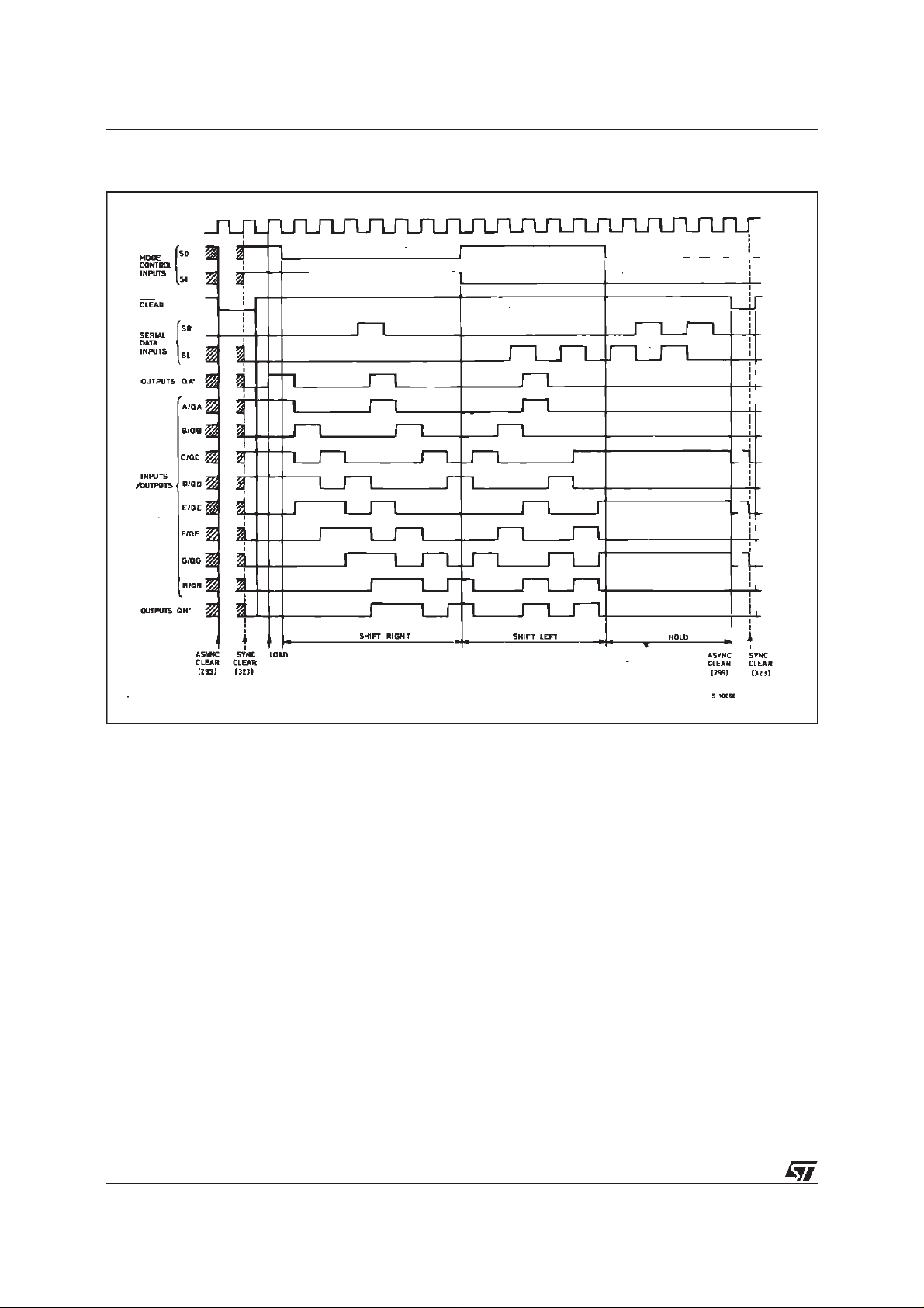
TIMINGCHART
4/13
 Loading...