

WITH 3-STATE OUTPUTS (NON INVERTED)
■ HIGH SPEED:
f
= 120MHz (TYP.) at VCC=5V
MAX
■ LOW POWER DISSIPATION:
I
=8µA(MAX.) at TA=25°C
CC
■ COMPATIBLE WITH TTL OUTPUTS
V
=2V(MIN.),VIL= 0.8V (MAX.)
IH
■ 50ΩTRANSMISSION LINE DRIVING
CAPABILITY
■ SYMMETRICAL OUTPUT IMPEDANCE:
|I
|=IOL= 24mA (M IN)
OH
■ OPERATING VOLTAGE RANGE:
V
(OPR) = 4.5V to 5. 5V
CC
■ IMPROVED LATCH-UP IMMUNITY
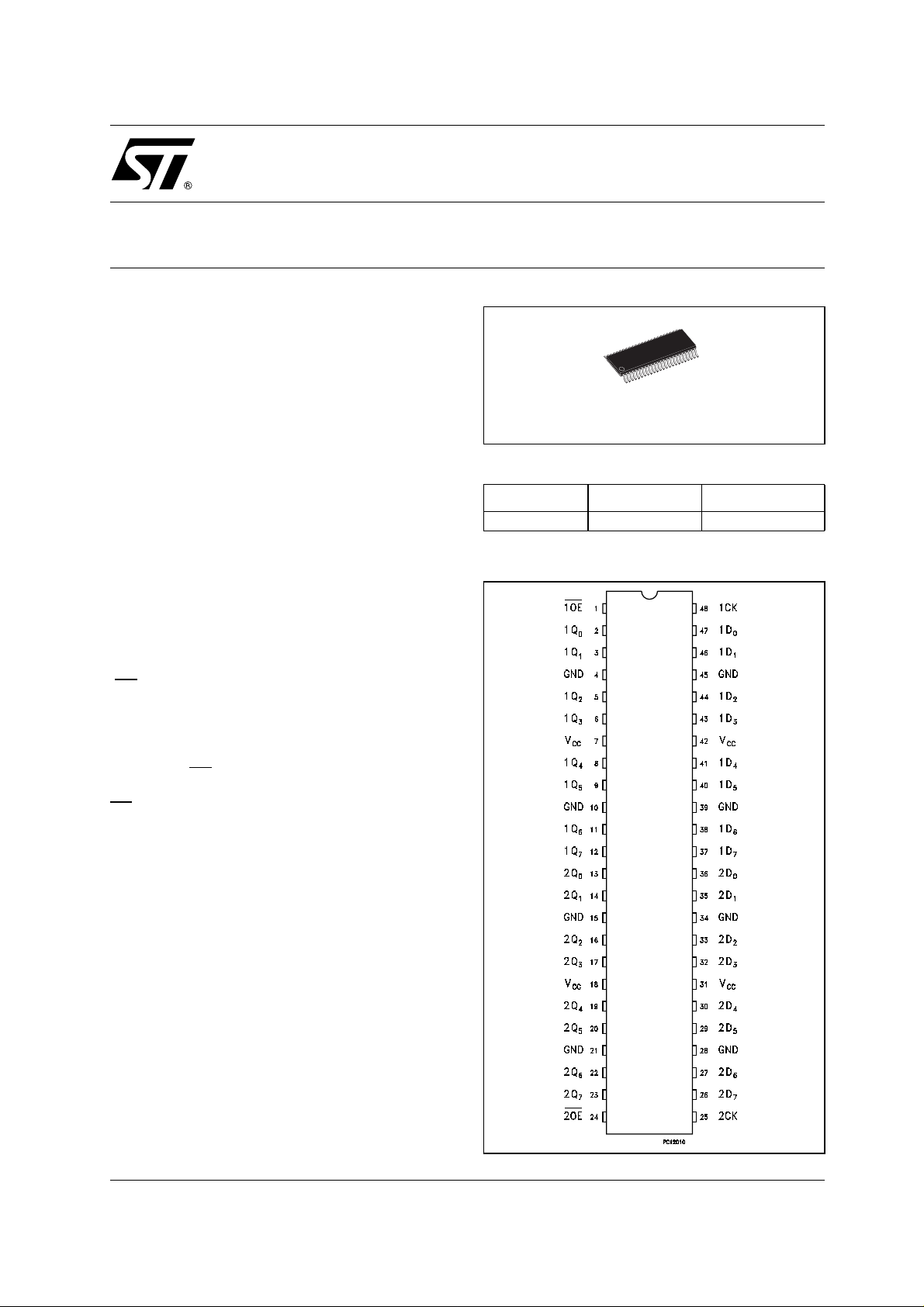
74ACT16374
16-BIT D-TYPE FLIP-FLOP
TSSOP
ORDER CODES
PACKAGE TUBE T & R
TSSOP 74ACT16374TTR
DESCRIPTION
The 74ACT16374 is an advanced high-speed
CMOS 16-BIT D-TYPE FLIP-FLOP (3-STATE)
fabricated with sub-micron silicon gate and
double-layer metal wiring C
2
MOS tecnology.
This 16 bit D-Type Flip-Flop is controlled by two
clock inputs (CK) and two output enable inputs
(OE
). The device can be used as two 8-bit
flip-flops or one 16-bit flip-flop.
On the positive transition of the clock, the Q
outputs will be set to the logic state th at were
setup at the D inputs.
While the (OE
) input is low , the outputs will be in
a normal logic sta te (high or low logic level); whil e
OE
is high, the outputs will be in a high impedance
state.
The output control does not affect the internal
operation of flip-flops; that is, the old data c an be
retained or the new data can be entered even
while the outputs are off.
All inputs and outputs are equipped with
protection circuits against static discharge, giving
them 2KV ESD immunity and t r ans ient excess
voltage.
PIN CONNE CTION
1/10February 2003
74ACT16374
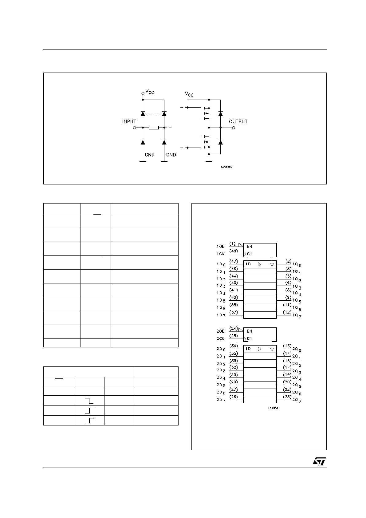
INPUT AND OUTPUT EQUIVALENT CIRCUIT
PIN DESCRIPTION
PIN No SYMBOL NAME AND FUNCTION
1 1OE
2, 3,5,6,8, 9,
11, 12
13,14,16, 17,
19, 20, 22, 23
24 2OE
25 2CK Clock Input (LOW-to-HIGH
36,35,33, 32,
30, 29, 27, 26
47,46,44, 43,
41, 40, 38, 37
48 1CK Clock Input (LOW-to-HIGH
4, 10, 15, 21,
28, 34, 39, 45
7, 18, 31, 42 V
1Q0 to
1Q7
2Q0 to
2Q7
2D0 to 2D7 Data Inputs
1D0 to 1D7 Data Inputs
GND Ground (0V)
3 State Output Enable
Input (Active LOW)
3-State Outputs
3-State Outputs
3 State Output Enable
Input (Active LOW)
Edge Trigger)
Edge Trigger)
Positive Supply Voltage
CC
TRUTH TABLE
INPUTS OUTPUT
*IEC LOGIC SYMBOLS
OE
HXX Z
L X NO CHANGE*
LLL
LHH
X : Don‘t Care
Z : High Impedance
2/10
CK D Q
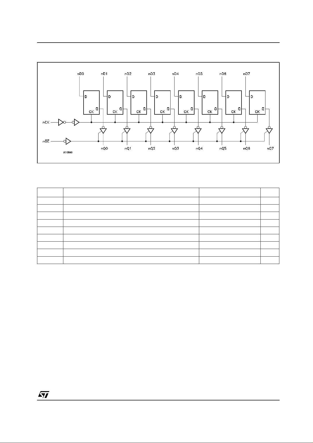
LOGIC DIAGRAM
This logic diagram has not to be used to estimate propagation delays
ABSOLUTE MAXIMUM RATINGS
74ACT16374
Symbol Parameter Value Unit
V
V
V
I
I
OK
I
or I
I
CC
T
T
Absolute Maximum Ratings are those values beyond which damage to the device may occur. Functional operation under these conditions is
not implied.
Supply Voltage
CC
DC Input Voltage -0.5 to VCC+ 0.5
I
DC Output Voltage -0.5 to VCC+ 0.5
O
DC Input Diode Current
IK
DC Output Diode Current
DC Output Current
O
DC VCCor Ground Current
GND
Storage Temperature
stg
Lead Temperature (10 sec)
L
-0.5 to +7 V
V
V
± 20 mA
± 20 mA
± 50 mA
± 400 mA
-65 to +150 °C
300 °C
3/10
 Loading...