

74ACT16373
16-BIT D-TYPE L ATCH
WITH 3-STATE OUTPUTS (NON INVERTED)
■ HIGH SPEED:t
■ LOW POWER DISSIPATION:
I
=8µA(MAX.) at TA=25°C
CC
■ COMPATIBLE WITH TTL OUTPUTS
V
=2V(MIN.),VIL= 0 .8V (MAX.)
IH
■ 50ΩTRANSMISSION LINE DRIVING
= 5.3ns (TYP.) at VCC=5V
PD
CAPABILITY
■ SYMMETRICAL OUTPUT IMPEDANCE:
|I
|=IOL= 24mA (MIN)
OH
■ OPERATING VOLTAGE RANGE:
V
(OPR) = 4.5V to 5.5V
CC
■ IMPROVED LATCH-UP IMMUNITY
DESCRIPTION
The 74ACT16373 is an advanced high-speed
CMOS 16-BIT D-TYPE LATCH (3-STATE)
fabricated with sub-micron silicon gate and
double-layer metal wiring C
2
MOS tecnology.
This 16 bit D-Type latch is controlled by two lat c h
enable inputs (LE) and two output enable inputs
(OE
). The dev ice can be used as two 8-bit latches
or one 16-bit latch.
While the LE input is held at a high level, the Q
outputs will follow the data inputs precisely. W hen
the LE is taken low, the Q outputs will be latched
precisely at the levels set up at the D inputs. While
the (OE
) input is low, the outputs will be in a
normal logic state (high or low logic level) and
while OE
is in high level the outputs will be in a
high impedance state.
This device is designed to interface directly High
Speed CMOS systems with TTL and NMOS
components.
All inputs and outpu ts are equipped with
protection circuits against static discharge, giving
them 2KV ESD im munity and transient excess
voltage.
TSSOP
ORDER CODES
PACKAGE TUBE T & R
TSSOP 74ACT16373TTR
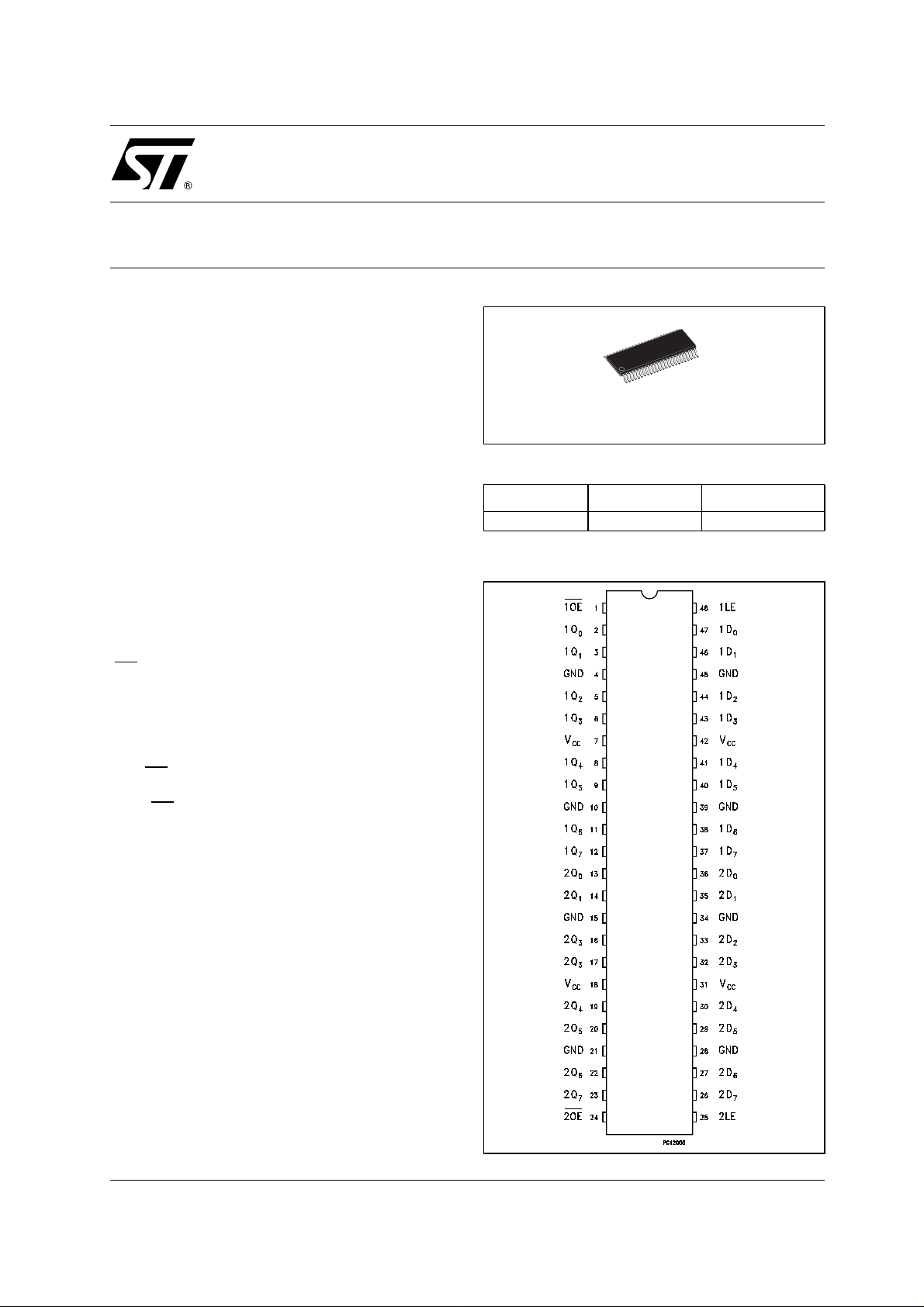
PIN CONNECTION
1/10February 2003
74ACT16373
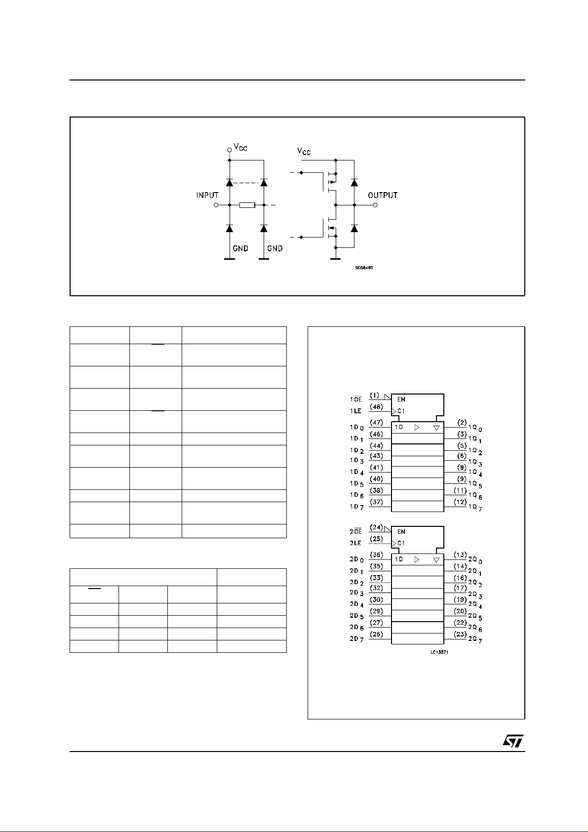
INPUT AND OUTPUT EQUIVALENT CIRCUIT
PIN DESCRIPTION
PIN No SYMBOL NAME AND FUNCTION
1 1OE
2, 3,5, 6,8,9,
11, 12
13,14,16,17,
19, 20, 22, 23
24 2OE
25 2LE Latch Enable Input
36,35,33,32,
30, 29, 27, 26
47,46,44,43,
41, 40, 38, 37
48 1LE Latch Enable Input
4, 10, 15, 21,
28, 34, 39, 45
7, 18, 31, 42 V
1Q0 to 1Q7 3-State Outputs
2Q0 to 2Q7 3-State Outputs
2D0 to 2D7 Data Inputs
1D0 to 1D7 Data Inputs
GND Ground (0V)
CC
3 State Output Enable
Input (Active LOW)
3 State Output Enable
Input (Active LOW)
Positive Supply Voltage
TRUTH TABLE
INPUTS OUTPUT
OE
HXX Z
L L X NO CHANGE *
LHL L
LHH H
X : Don‘tCare
Z : High Impedance
* : Q outputs are latched atthetimewhenthe LEinputistakenlow
logic level.
LE D Q
IEC LOGIC SYMBOLS
2/10
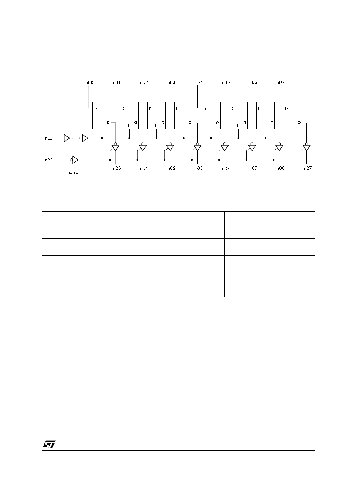
LOGIC DIAGRAM
This logic diagram has not to be used to estimate propagation delays
ABSOLUTE MAXIMUM RATINGS
74ACT16373
Symbol Parameter Value Unit
V
V
V
I
I
OK
I
or I
I
CC
T
T
Absolute Maximum Ratings are those values beyond which damage to the device may occur. Functional operation under these conditions is
not implied.
Supply Voltage
CC
DC Input Voltage -0.5 to VCC+ 0.5
I
DC Output Voltage -0.5 to VCC+ 0.5
O
DC Input Diode Current
IK
DC Output Diode Current
DC Output Current
O
DC VCCor Ground Current
GND
Storage Temperature
stg
Lead Temperature (10 sec)
L
-0.5 to +7 V
V
V
± 20 mA
± 20 mA
± 50 mA
± 400 mA
-65 to +150 °C
300 °C
3/10

74ACT16373
RECOMMENDED OPERATING CONDITIONS
Symbol Parameter Value Unit
V
V
V
T
dt/dv
1) VINfrom0.8V to 2.0V
DC SPECIFICATIONS
Symbol Parameter
V
IH
V
IL
V
OH
V
OL
I
I
I
OZ
I
CCT
I
CC
I
OLD
I
OHD
1) Maximum test duration 2ms, one output loaded at time
2) Incident wave switching is guaranteed on transmission lines with impedances as low as 50Ω
Supply Voltage
CC
Input Voltage 0 to V
I
Output Voltage 0 to V
O
Operating Temperature
op
Input Rise and Fall Time V
= 4.5 to 5.5V (note 1)
CC
Test Condition Value
= 25°C
T
A
Min. Typ. Max. Min. Max. Min. Max.
2.0 1.5 2.0 2.0
1.5 0.8 0.8 0.8
4.4 4.49 4.4 4.4
5.4 5.49 5.4 5.4
3.86 3.76 3.7
4.86 4.76 4.7
0.001 0.1 0.1 0.1
0.001 0.1 0.1 0.1
0.36 0.44 0.5
0.36 0.44 0.5
± 0.1 ± 1 ± 1 µA
± 0.5 ± 5 ± 10 µA
0.6 1.5 1.6 mA
880160µA
High Level Input
Voltage
Low Level Input
Voltage
High Level Output
Voltage
Low Level Output
Voltage
Input Leakage Current
High Impedance
Output Leakege
Current
Max ICC/Input
Quiescent Supply
Current
Dynamic Output
Current (note 1, 2)
V
CC
(V)
4.5 VO= 0.1 V or
-0.1V
V
CC
4.5 VO= 0.1 V or
V
5.5 1.5 0.8 0.8 0.8
4.5
5.5
4.5
5.5
4.5
5.5
4.5
5.5
V
5.5
5.5
VO=VCCor GND
5.5
V
5.5
V
5.5
V
-0.1V
CC
IO=-50 µA
=-50 µA
I
O
=-24 mA
I
O
=-24 mA
I
O
IO=50 µA
=50 µA
I
O
=24 mA
I
O
=24 mA
I
O
I=VIH
or GND
orV
I=VCC
V
VI=VCC- 2.1V
I=VCC
OLD
OHD
or GND
= 1.65 V max
= 3.85 V min
IL
4.5 to 5.5 V
CC
CC
-55 to 125 °C
8 ns/V
-40 to 85°C -55 to 125°C
75 50 mA
-75 -50 mA
V
V
Unit
V5.5 2.0 1.5 2.0 2.0
V
V
4/10

AC ELECTRICAL CHARACTERISTICS (CL=50pF,RL= 500 Ω, Input tr=tf=3ns)
Test Condition Value
= 25°C
Symbol Parameter
t
t
t
t
t
t
PZH
t
t
PHZ
t
W(H)
(*) Voltage range is 5.0V± 0.5V
Propagation Delay
PLH
Time LE to Q
PHL
Propagation Delay
PLH
Time D to Q
PHL
Output Enable
PZL
Time
Output Disable
PLZ
Time
LE Minimum Pulse
Width HIGH
Setup Time D to
t
s
LE, HIGH or LOW
Hold Time D to LE,
t
h
HIGH or LOW
V
(V)
5.0
5.0
5.0
5.0
5.0
5.0
5.0
CC
T
A
Min. Typ. Max. Min. Max. Min. Max.
(*)
4.2 6.5 12.8 13.7
5.0 7.7 12.2 13.0
(*)
4.1 6.3 11.1 11.8
5.3 8.5 12.3 13.0
(*)
5.7 6.5 14.2 15.1
5.0 7.7 12.1 13.0
(*)
5.6 8.2 9.4 9.8
5.0 7.0 10.7 11.0
(*)
(*)
(*)
2.2 1.7 2.6 2.6
1.2 <1.0 1.4 1.4
1.3 <1.0 1.6 1.6
-40 to 85°C -55 to 125°C
74ACT16373
Unit
ns
ns
ns
ns
ns
ns
ns
CAPACITIVE CHARACTERISTICS
Test Condition Value
= 25°C
Symbol Parameter
V
CC
(V)
C
C
C
1) CPDis defined as the value of the IC’s internal equivalent capacitance which is calculated from the operating current consumption without
load. (Refer to Test Circuit). Average operating current can be obtained by the following equation. I
circuit)
Input Capacitance
IN
Output Capaci-
OUT
tance
Power Dissipation
PD
Capacitance (note1)5.0
5.0 3.5 pF
5.0 11 pF
= 10MHz
f
IN
T
A
Min. Typ. Max. Min. Max. Min. Max.
31 pF
-40 to 85°C -55 to 125°C
CC(opr)=CPDxVCCxfIN+ICC
Unit
/16 (per
5/10

74ACT16373
TEST CIRCUIT
Test Switch
t
PLH,tPHL
t
PZL,tPLZ
t
PZH,tPHZ
CL= 50pF or equivalent (includes jig and probe capacitance)
R
=500Ωor equivalent
L=R1
R
T=ZOUT
of pulse generator (typically 50Ω)
Open
2V
CC
GND
WAVEFORM 1: PRO PAGAT ION DELAYS, PULSE WIDTH, SETUP AND HOLD TIMES (f=1MHz; 50%
duty cycle)
6/10

WAVEFORM 2: OUTPUT ENABLE AND DISABLE TIMES (f=1MHz; 5 0% duty cycle)
74ACT16373
WAVEFORM 3: PROPAGATION DELAYS TIME (f=1MHz; 50% duty cycle)
7/10

74ACT16373
TSSOP48 MECHANICAL DATA
mm. inch
DIM.
MIN. TYP MAX. MIN. TYP. MAX.
A 1.2 0.047
A1 0.05 0.15 0.002 0.006
A2 0.9 0.035
b 0.17 0.27 0.0067 0.011
c 0.09 0.20 0.0035 0.0079
D 12.4 12.6 0.488 0.496
E 8.1 BSC 0.318 BSC
E1 6.0 6.2 0.236 0.244
e 0 .5 BSC 0.0197 BSC
K0˚ 8˚0˚ 8˚
L 0.50 0.75 0.020 0.030
A2
A
A1
b
e
D
K
c
E1
L
E
PIN 1 IDENTIFICATION
8/10
1
7065588C

74ACT16373
Tape & Reel TSSOP48 MECHANICAL DATA
mm. inch
DIM.
MIN. TYP MAX. MIN. TYP. MAX.
A 330 12.992
C 12.8 13.2 0.504 0.519
D 20.2 0.795
N 60 2.362
T 30.4 1.197
Ao 8.7 8.9 0.343 0.350
Bo 13.1 13.3 0.516 0.524
Ko 1.5 1.7 0.059 0.067
Po 3.9 4.1 0.153 0.161
P 11.9 12.1 0.468 0.476
9/10

74ACT16373
Information furnished is believed to be accurate and reliable. However, STMicroelectronics assumes no responsibility for the
consequences of use o f suc h inf ormat ion n or f or an y infr ingeme nt of paten ts or oth er ri gh ts of third part ies whic h may resul t f rom
its use. No license is granted by implication or otherwise under any patent or patent rights of STMicroelectronics. Specifications
mentioned in this publication are subject to change without notice. This publication supersedes and replaces all information
previously supplied. STMicroelectronics products are not authorized for use as critical components in life support devices or
systems without express written approval of STMicroelectronics.
Australia - Brazil - Canada - China - Finland - France - Germany - Hong Kong - India - Israel - Italy - Japan - Malaysia - Malta - Morocco
© The ST logo is a registered trademark of STMicroelectronics
© 2003 STMicroelectronics - Printed in Italy - All Rights Reserved
STMicroelectronics GROUP OF COMPANIES
Singapore - Spain - Sweden - Switzerland - United Kingdom - United States.
© http://www.st.com
10/10
 Loading...