74ACT16245
16-BIT BUS TRANSCEIVER
WITH 3-STATE OUTPUTS (NON INVERTED)
■ HIGH SPEED: t
■ LOW POWER DISSIPATION:
I
=8µA(MAX.) atTA=25°C
CC
■ COMPATIBLE WITHTTL OUTPUTS
V
=2V(MIN.),VIL= 0.8V (MAX.)
IH
■ 50ΩTRANSMISSION LINE DRIVING
= 4.9ns (TYP.) at VCC=5V
PD
CAPABILITY
■ SYMMETRICAL OUTPUT IMPEDANCE:
|I
|=IOL= 24mA (MIN)
OH
■ OPERATING VOLTAGE RANGE:
V
(OPR) = 4.5V to 5.5V
CC
■ IMPROVED LATCH-UP IMMUNITY
DESCRIPTION
The 74ACT16245 is an advanced high-speed
CMOS 16-BIT BUS TRANSCEIVER (3-STATE)
fabricated with sub-micron silicon gate and
double-layer metal wiring C
2
MOS technology.
This IC is intended f or two-way asyn ch ronous
communication between data buses and the
direction of data transmission is determined by
DIR input. The enable inputs G
can be used to
disable the device so that the buses are effectively
isolated.
All floating bus terminals during the Z-s tate must
be held HIGH or LOW.
All inputs and outputs are e quipped w ith protection circuits against static disc harge, giving t hem
2KV ESD immunity and transient excess voltage.
TSSOP
ORDER CODES
PACKAGE TUBE T & R
TSSOP 74ACT16245TTR
PIN CONNECTION
1/9July 2003

74ACT16245
INPUT AND OUTPUT EQUIVALENT CIRCUIT
PIN DESCRIPTION
PIN No SYMBOL NAME AND FUNCTION
1 1DIR Directional Control
2, 3, 5, 6, 8, 9,
11, 12
13,14,16,17,
19, 20, 22, 23
24 2DIR Directional Control
25 2G
36,35,33,32,
30, 29, 27, 26
47,46,44,43,
41, 40, 38, 38
48 1G
4, 10, 15, 21,
28, 34, 39, 45
7, 18, 31, 42
1B1 to 1B8 Data Inputs/Outputs
2B1 to 2B8 Data Inputs/Outputs
Output Enable Input
2A1 to 2A8 Data Inputs/Outputs
1A1 to 1A8 Data Inputs/Outputs
Output Enable Input
GND Ground (0V)
V
CC
Positive Supply Voltage
TRUTH TABLE
INPUTS FUNCTION OUTPUT
G
L L OUTPUT INPUT A = B
L H INPUT OUTPUT B = A
HXZZZ
X : Don‘tCare
Z : High Impedance
DIR A BUS B BUS Yn
IEC LOGIC SYMBOLS
2/9

74ACT16245
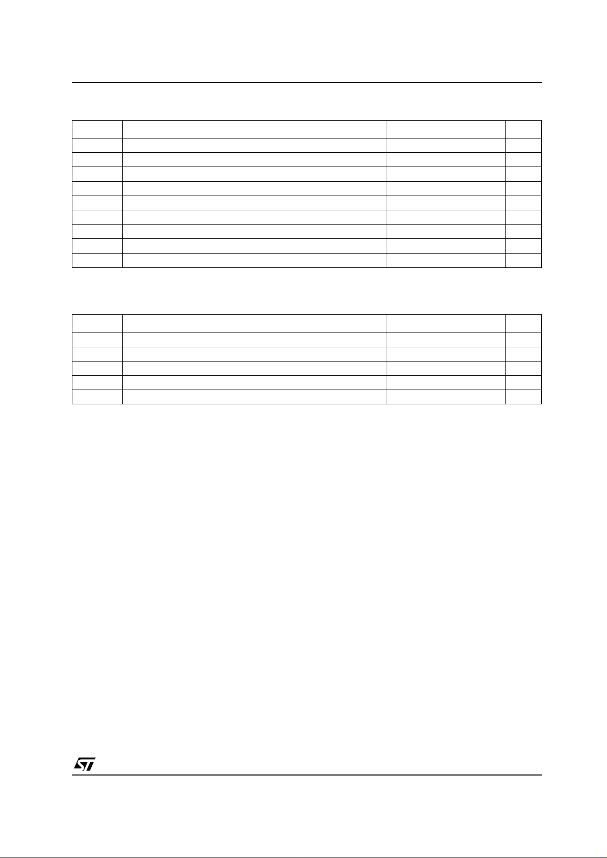
ABSOLUTE MAXIMUM RATINGS
Symbol Parameter Value Unit
V
V
V
I
I
OK
I
or I
I
CC
T
T
Absolute Maximum Ratings are those values beyond which damage to the device may occur. Functional operation under these conditions is
not implied.
RECOMMENDED OPERATING CONDITIONS
Symbol Parameter Value Unit
V
V
V
T
dt/dv
1) VINfrom0.8V to 2.0V
Supply Voltage
CC
DC Input Voltage -0.5 to VCC+ 0.5
I
DC Output Voltage -0.5 to VCC+ 0.5
O
DC Input Diode Current
IK
DC Output Diode Current
DC Output Current
O
DC VCCor Ground Current
GND
Storage Temperature
stg
Lead Temperature (10 sec)
L
Supply Voltage
CC
Input Voltage 0 to V
I
Output Voltage 0 to V
O
Operating Temperature
op
Input Rise and Fall Time V
= 4.5 to 5.5V (note 1)
CC
-0.5 to +7 V
± 20 mA
± 20 mA
± 50 mA
± 400 mA
-65 to +150 °C
300 °C
4.5 to 5.5 V
CC
CC
-55 to 125 °C
8 ns/V
V
V
V
V
3/9
 Loading...