

SGS Thomson Microelectronics 74ACT158 Datasheet

QUAD 2 CHANNEL MULTIPLEXER (INV.)
■ HIGH SPEED:t
■ LOWPOWERDISSIPATION:
=8µA (MAX.)at TA=25oC
I
CC
■ COMPATIBLEWITH T TLOUTPUTS
V
=2V(MIN),VIL= 0.8V (MAX)
IH
■ 50Ω TRANSMISSIONLINE DRIVING
CAPABILITY
■ SYMMETRICAL OUTPUT IMPEDANCE:
|I
|=IOL=24mA(MIN)
OH
■ BALANCED PROPAGATIONDELAYS:
t
≅ t
PLH
PHL
■ OPERATINGVOLTAGERANGE:
V
(OPR)= 4.5V to 5.5V
CC
■ PIN AND FUNCTION COMPATIBLE WITH
74SERIES158
■ IMPROVED LATCH-UP IMMUNITY
DESCRIPTION
The ACT158 is an high-speed CMOS QUAD
2-CHANNEL MULTIPLEXER fabricated with
sub-micron silicon gate and double-layer metal
wiring C
2
MOS technology. It is ideal for low
power applications maintaining high speed
operation similar to equivalent Bipolar Schottky
TTL.
It consists of four 2-input digital multiplexers with
=4 ns(TYP.)atVCC=5V
PD
74ACT158
PRELIMINARY DATA
B
(Plastic Package)
(Micro Package)
ORDERCODES:
74ACT158B 74ACT158M
common select and strobe inputs. It is an
inverting multiplexer. When the STROBE input is
held High selection of data is inhibit and all the
outputs become high. The SELECT decoding
determines whether the A or B inputs get routed
to theircorresponding Y outputs.
The device is designed to interface directly High
Speed CMOS systems with TTL, NMOS and
CMOSoutput voltagelevels.
All inputs and outputs are equipped with
protectioncircuits against static discharge, giving
them 2KV ESD immunity and transient excess
voltage.
M
PINCONNECTION ANDIEC LOGICSYMBOLS
May 1997
1/8
74ACT158
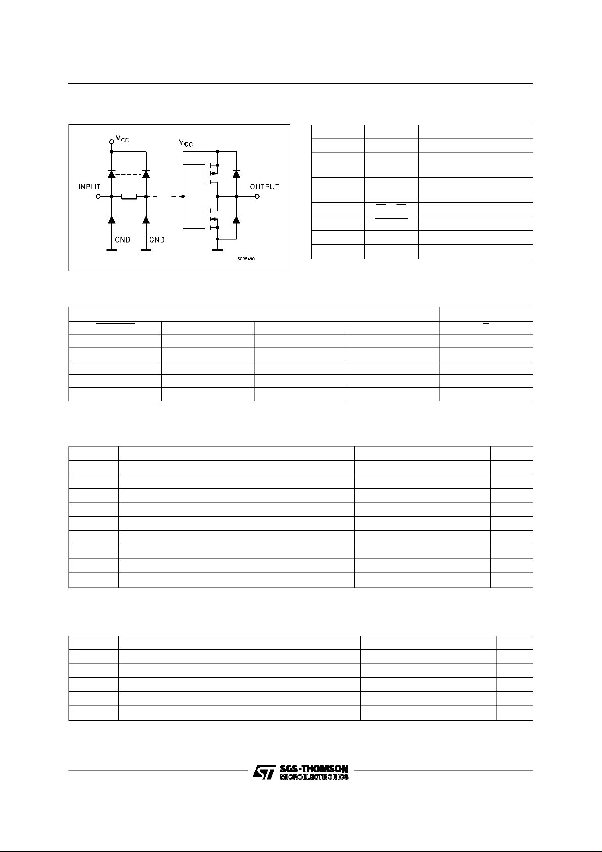
INPUTAND OUTPUT EQUIVALENTCIRCUIT
PIN DESCRIPTION
PI N No SYM B O L NAME AND F UNCTION
1 SELECT Common Data Select Input
2,5,11,14 1Ato4A Data Inputs From
Source A
3,6,10,13 1Bto4B Data Inputs From
Source B
4,7,9,12 1Yto4Y Multiplexer Outputs
15 STROBE Strobe Input
8 GND Ground (0V)
16 V
CC
Positive Supply Voltage
TRUTH TABLE
INPUT OUTPUT
ST RO B E SEL ECT A B Y
HXXXH
LLLXH
LLHXL
LHXLH
LHXHL
X:”H”or ”L”
ABSOLUTE MAXIMUM RATING
Symb o l Parame t er Val u e Uni t
V
V
V
I
I
OK
I
orI
I
CC
T
T
Absolute Maximum Ratings are those values beyond which d amage to the device may occur. Functional operation under these condition isnot implied.
Supply Voltage -0.5to+7 V
CC
DC Input Voltage -0.5toVCC+0.5 V
I
DC Output Voltage -0.5toVCC+0.5 V
O
DC Input Diode Current ± 20 mA
IK
DC Output Diode Current ± 20 mA
DC Output Current ± 50 mA
O
DC VCCor Ground Current ± 200 mA
GND
Storage Temperature -65to+150
stg
Lead Temperature (10 sec) 300
L
o
C
o
C
RECOMMENDED OPERATINGCONDITIONS
Symbol Parameter Valu e Unit
V
V
V
T
dt/dv Input Rise and Fall Time V
1) VINfrom0.8Vto2.0V
Supply Voltage 4.5to5.5 V
CC
Input Voltage 0toV
I
Output Voltage 0toV
O
Operating Temperature: -40to+85
op
= 4.5 to 5.5V (note 1) 8 ns/V
CC
CC
CC
V
V
o
C
2/8
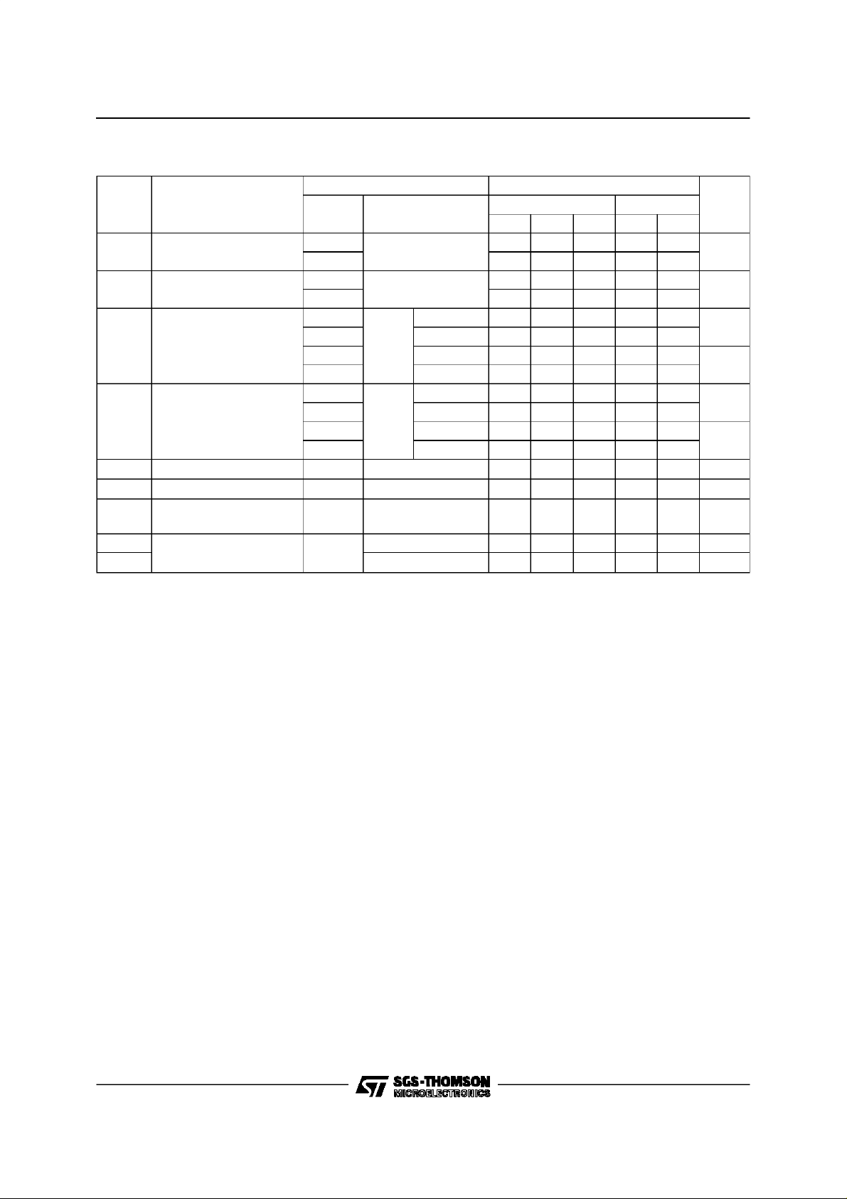
DC SPECIFICATIONS
74ACT158
Symbol Parameter Test Condition s Value Unit
=25oC-40to85
V
CC
(V)
High Level Input Voltage 4.5 VO=0.1V or
V
IH
5.5 2.0 1.5 2.0
Low Level Input Voltage 4.5 VO=0.1V or
V
IL
5.5 1.5 0.8 0.8
High Level Output
V
OH
Voltage
4.5
5.5 I
4.5 I
5.5 I
Low Level Output
V
OL
Voltage
4.5
5.5 I
4.5 I
5.5 I
Input Leakage Current
I
I
Max ICC/Input 5.5 VI=VCC-2.1V 0.6 1.5 mA
I
CCT
Quiescent Supply
I
CC
5.5
5.5 VI=VCCorGND 8 80 µA
V
-0.1V
CC
-0.1V
V
CC
IO=-50µA 4.4 4.49 4.4
(*)
=
V
I
or
V
IH
V
IL
(*)
V
I
V
or
IH
V
IL
=-50µA 5.4 5.49 5.4
O
=-24 mA 3.86 3.76
O
=-24 mA 4.86 4.76
O
IO=50µA0.0010.1 0.1
=
=50 mA 0.001 0.1 0.1
O
=24mA 0.36 0.44
O
=24mA 0.36 0.44
O
VI=VCCorGND ±0.1 ±1 µA
T
A
Min. Typ. Max. Min. Max.
2.0 1.5 2.0
1.5 0.8 0.8
o
C
Current
Dynamic Output Current
I
OLD
(note 1, 2)
I
OHD
1) Maximum test duration 2ms, one output loaded at time
2) Incident wave switching isguaranteed on transmission lines with impedances as low as 50 Ω.
(*)All outputs loaded.
5.5 V
=1.65 Vmax 75 mA
OLD
V
=3.85Vmin -75 mA
OHD
V
V
V
V
3/8
 Loading...