

74ACT14
HEX SCHMITT INVERTER
■ HIGHSPEED:t
■
LOW POWER DISSIPATION:
I
=4 µA (MAX.)at TA=25oC
CC
■
50ΩTRANSMISSIONLINEDRIVING
=5ns (TYP.)atVCC=5V
PD
CAPABILITY
■ SYMMETRICALOUTPUTIMPEDANCE:
|=IOL=24mA(MIN)
|I
OH
■ BALANCEDPROPAGATIONDELAYS:
t
≅ t
PLH
PHL
■ OPERATINGVOLTAGERANGE:
V
(OPR)= 2Vto5V
CC
■
PINANDFUNCTIONCOMPATIBLEWITH
74SERIES14
■ IMPROVEDLATCH-UPIMMUNITY
DESCRIPTION
The ACT14 is an advanced high-speed CMOS
HEX SCHMITT INVERTER fabricated with
sub-micron silicon gate and double-layer metal
wiring C
2
MOS technology. It is ideal for low
power applications mantaining high speed
operation similar to equivalent Bipolar Shottky
TTL.
The internal circuit is composed of 3 stages
including buffer output, which enables high noise
B
(PlasticPackage)
(Micro Package)
M
ORDERCODES :
74ACT14B 74ACT14M
immunityand stableoutput.
The device is designed to interface directly High
Speed CMOS systems with TTL, NMOS and
CMOSoutput voltagelevels
This together with its schmitt trigger function
allows it to be used on line receivers with slow
rise/fallinput signals.
All inputs and outputs are equipped with
protection circuits against static discharge, giving
them 2KV ESD immunity and transient excess
voltage.
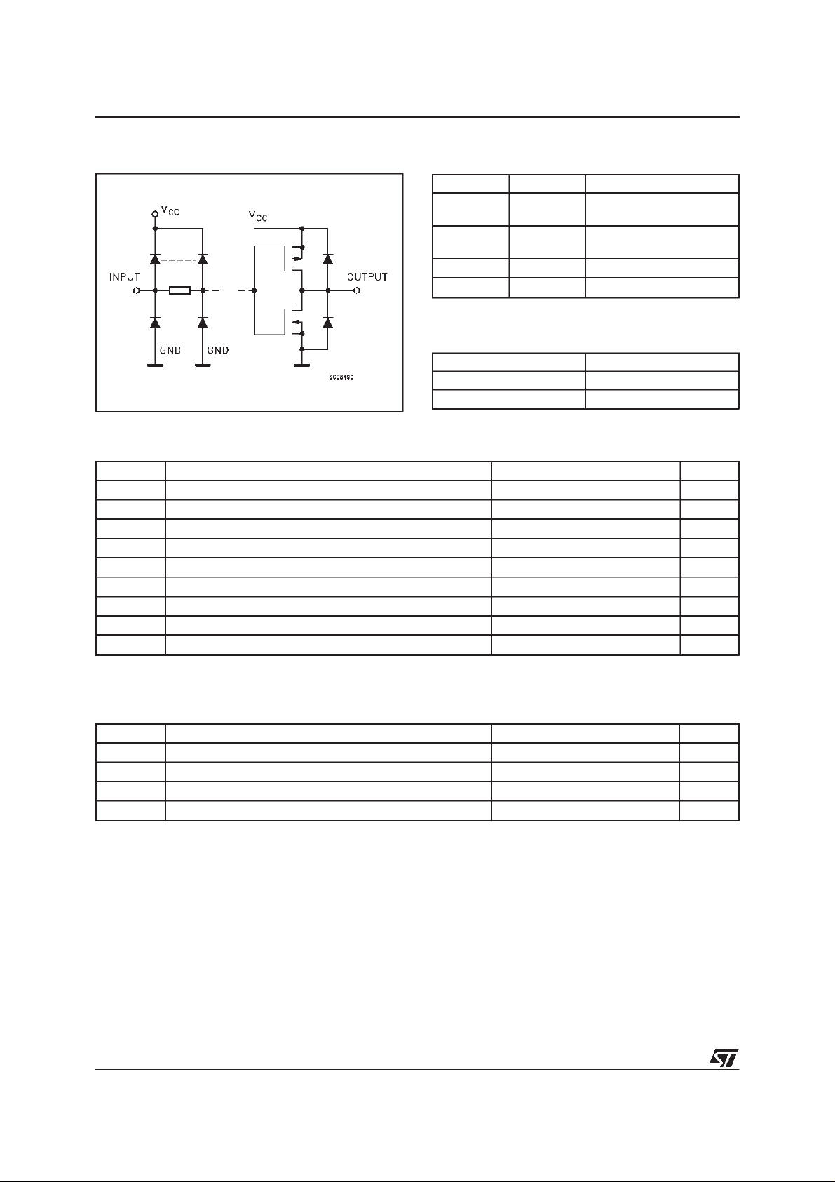
PIN CONNECTION AND IEC LOGICSYMBOLS
March 1999
1/7
74ACT14
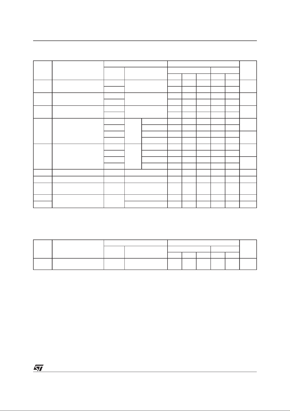
INPUT AND OUTPUTEQUIVALENTCIRCUIT
PIN DESCRIPTION
PI N No SYMB OL NAME AND FUNCT I O N
1, 3, 5, 9,
1A to 6A Data Inputs
11, 13
2, 4, 6, 8,
1Y to 6Y Data Outputs
10, 12
7 GND Ground (0V)
14 V
CC
Positive Supply Voltage
TRUTH TABLE
AY
LH
HL
ABSOLUTE MAXIMUM RATINGS
Symb o l Para met er Val u e Uni t
V
V
V
I
I
OK
I
or I
I
CC
T
T
AbsoluteMaximumRatingsarethosevaluesbeyondwhichdamageto thedevicemayoccur.Functionaloperationunderthesecondition isnotimplied.
Supply Voltage -0.5 to +7 V
CC
DC Input Voltage -0.5 to VCC+ 0.5 V
I
DC Output Voltage -0.5 to VCC+ 0.5 V
O
DC Input Diode Current
IK
DC Output Diode Current
DC Output Current ± 50 mA
O
DC VCCor Ground Current ± 300 mA
GND
Storage Temperature -65 to +150
stg
Lead Temperature (10 sec) 300
L
20 mA
±
20 mA
±
o
C
o
C
RECOMMENDED OPERATINGCONDITIONS
Symb o l Para met er Value Un it
V
V
V
T
2/7
Supply Voltage 2 to 6 V
CC
Input Voltage 0 to V
I
Output Voltage 0 to V
O
Operating Temperature: -40 to +85
op
CC
CC
V
V
o
C
74ACT14
DC SPECIFICATIONS
Symbol Parameter Test Conditions Value Unit
T
V
CC
(V)
High Level Input Voltage 4.5 2.0 2.0
V
t+
5.5 2.0 2.0
Low Level Input Voltage 4.5 0.6 0.6
V
t-
5.5 0.6 0.6
Hysteresis Voltage 4.5 0.4 1.4 0.4 1.4
V
h
5.5 0.4 1.5 0.4 1.5
High Level Output
V
OH
Voltage
Low Level Output
V
OL
Voltage
Input Leakage Current
I
I
Max ICC/Input 5.5 VI=VCC-2.1V 0.6 1.5 mA
I
CCT
Quiescent Supply
I
CC
4.5
5.5 I
4.5 I
V
I
V
IH
V
5.5 I
4.5
5.5 I
4.5 I
V
I
V
IH
V
5.5 I
5.5
VI=VCCor GND
IO=-50 µA 4.4 4.49 4.4
(*)
=
=-50µA 5.4 5.49 5.4
O
or
IL
(*)
IL
=-24 mA 3.86 3.76
O
=-24 mA 4.86 4.76
O
IO=50 µA 0.001 0.1 0.1
=
=50 mA 0.001 0.1 0.1
O
or
=24 mA 0.36 0.44
O
=24 mA 0.36 0.44
O
5.5 VI=VCCor GND 4 40 µA
Current
Dynamic Output Current
I
OLD
OHD
(note 1, 2)
I
1) Maximumtest duration 2ms, one output loaded at time
2)Incident waveswitchingisguaranteed ontransmission lineswithimpedancesaslow as50Ω.
(*)All outputs loaded.
5.5 V
= 1.65 V max 75 mA
OLD
V
= 3.85 V min -75 mA
OHD
=25oC -40 to 85oC
A
Min. Typ. Max. Min. Max.
0.1
±
1
±
µ
V
V
V
V
V
A
AC ELECTRICAL CHARACTERISTICS
= 50 pF,RL= 500 Ω, Input tr=tf=3 ns)
(C
L
Symbol Parameter Test Condition Value Unit
t
Propagation Delay Time 5.0
PLH
t
PHL
(*) Voltagerangeis 5V± 0.5V
V
(V)
CC
(*)
T
=25oC -40 to 85oC
A
Min. Typ. Max. Min. Max.
7.2 11.4 13.0 ns
3/7

74ACT14
CAPACITIVE CHARACTERISTICS
Symbol Parameter Test Conditions Value Unit
T
V
CC
(V)
Input Capacitance
C
IN
Power Dissipation
C
PD
5.0
5.0 30 pF
Capacitance (note 1)
1)CPDisdefined asthevalue oftheIC’sinternal equivalentcapacitance whichis calculated fromtheoperatingcurrentconsumption without load.(Referto
TestCircuit).Average operatingcurrent canbeobtainedbythefollowingequation.I
(opr)= CPD• VCC• fIN+ICC/6(percircuit)
CC
TESTCIRCUIT
=25oC -40 to 85oC
A
Min. Typ. Max. Min. Max.
510 10
pF
CL= 50 pF or equivalent (includes jigand probe capacitance)
=500Ωorequivalent
R
L=R1
R
ofpulse generator (typically50Ω)
T=ZOUT
WAVEFORM:PROPAGATIONDELAYS (f=1MHz)
4/7

Plastic DIP-14 MECHANICAL DATA
74ACT14
DIM.
MIN. TYP. MAX. MIN. TYP. MAX.
a1 0.51 0.020
B 1.39 1.65 0.055 0.065
b 0.5 0.020
b1 0.25 0.010
D 20 0.787
E 8.5 0.335
e 2.54 0.100
e3 15.24 0.600
F 7.1 0.280
I 5.1 0.201
L 3.3 0.130
Z 1.27 2.54 0.050 0.100
mm inch
P001A
5/7

74ACT14
SO-14 MECHANICALDATA
DIM.
MIN. TYP. MAX. MIN. TYP. MAX.
A 1.75 0.068
a1 0.1 0.2 0.003 0.007
a2 1.65 0.064
b 0.35 0.46 0.013 0.018
b1 0.19 0.25 0.007 0.010
C 0.5 0.019
c1 45 (typ.)
D 8.55 8.75 0.336 0.344
E 5.8 6.2 0.228 0.244
e 1.27 0.050
e3 7.62 0.300
F 3.8 4.0 0.149 0.157
G 4.6 5.3 0.181 0.208
L 0.5 1.27 0.019 0.050
M 0.68 0.026
S 8 (max.)
mm inch
6/7
P013G

74ACT14
Information furnished is believed tobeaccurate and reliable. However, STMicroelectronics assumes no responsibility for the consequences
of use of such information nor for any infringement of patents or other rights of third parties which may result from its use. No license is
granted by implication or otherwise under any patent or patent rights of STMicroelectronics. Specification mentioned in this publication are
subject tochange without notice. This publication supersedes and replaces all information previously supplied. STMicroelectronics products
are not authorized for use as critical components inlife support devices or systems without express written approval of STMicroelectronics.
The ST logo is a trademark of STMicroelectronics
1999 STMicroelectronics – Printed in Italy – All Rights Reserved
STMicroelectronics GROUP OF COMPANIES
Australia - Brazil - Canada - China -France - Germany - Italy - Japan -Korea - Malaysia -Malta - Mexico -Morocco - The Netherlands -
Singapore - Spain -Sweden - Switzerland - Taiwan - Thailand - United Kingdom -U.S.A.
http://www.st.com
.
7/7
 Loading...