

SGS Thomson Microelectronics 74ACT00MTR, 74ACT00M, 74ACT00B, 74ACT00TTR Datasheet
74ACT00
QUAD 2-INPUT NAND GATE
■ HIGH SPEED: t
■ LOW POWER DISSIPATION:
I
= 2µA(MAX.) at TA=25°C
CC
■ COMPA TIBLE WITH TTL OUTPUTS
V
= 2V (MIN.), VIL = 0.8V (MAX.)
IH
■ 50Ω TRANSMISSION LINE DRIVING
= 4.5ns (TYP.) at VCC = 5V
PD
CAPABILITY
■ SYMMETRICAL OUTPUT IMPEDANCE:
|I
| = IOL = 24mA (MIN)
OH
■ BALANCED PROPAGATION DELAYS:
t
≅ t
PLH
■ OPERATING VOL TAGE RANGE:
V
CC
■ PIN AND FUNCTION COMPATIBLE WITH
PHL
(OPR) = 4.5V to 5.5V
74 SERIES 00
■ IMPROVED LATCH-UP IMMUNITY
DESCRIPTION
The 74ACT00 is an advanced high-speed CMOS
QUAD 2-INPUT NAND GATE fabricated with
sub-micron silicon gate and double-layer metal
wiring C
2
MOS tecnology.
The internal circuit is composed of 3 stages
including buffer output , which enables high noise
TSSOPDIP SOP
ORDER CODES
PACKAGE TUBE T & R
DIP 74ACT00B
SOP 74ACT00M 74ACT00MTR
TSSOP 74ACT00TTR
immunity and stable output.
The device is designed to interface directly High
Speed CMOS systems with TTL, NMOS and
CMOS output voltage levels.
All inputs and outputs are equipped with
protection circuits against stat ic discharge, giving
them 2KV ESD immunity and transient excess
voltage.
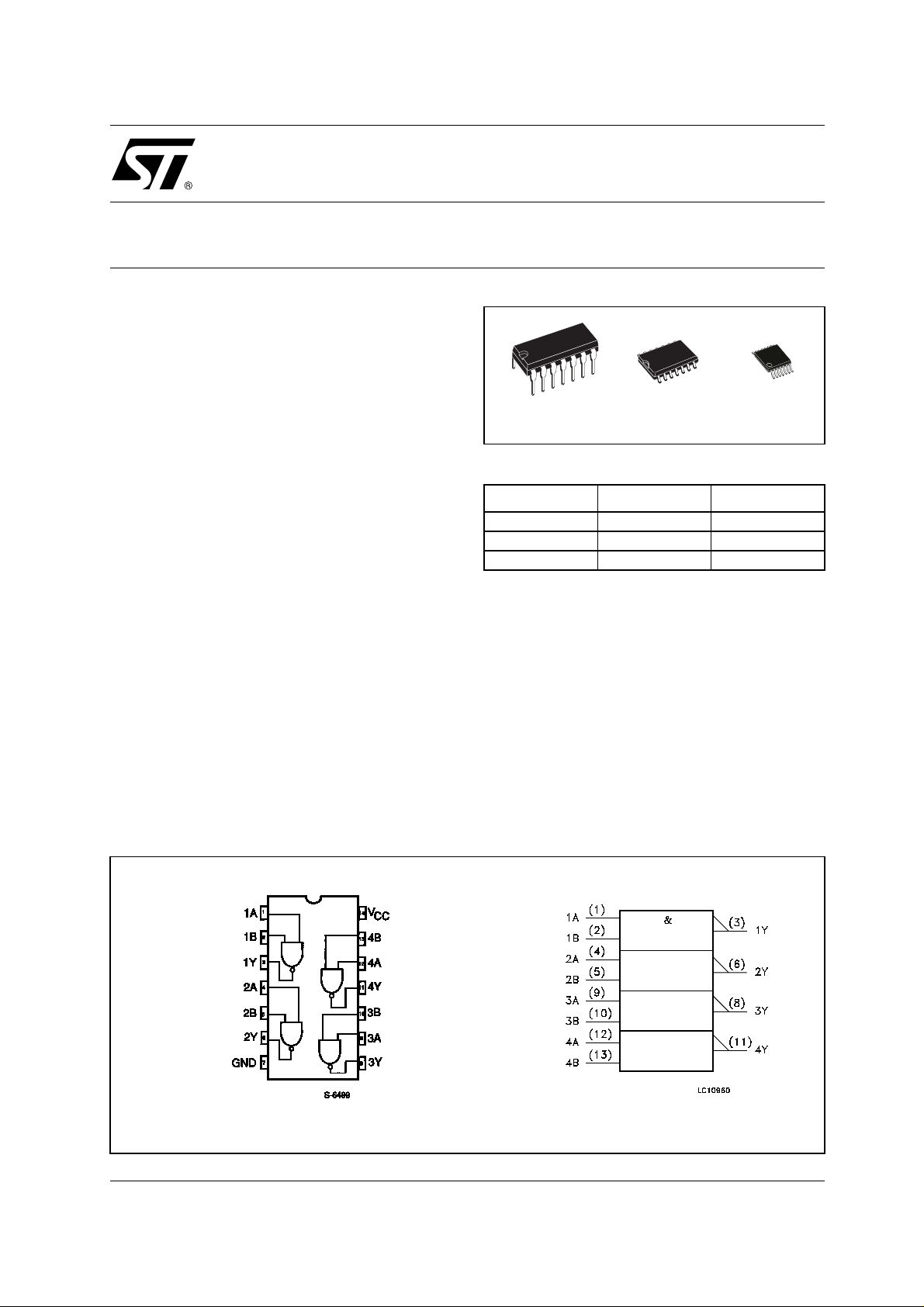
PIN CONNECTION AND IEC LOGIC SYMBOLS
1/8April 2001
74ACT00
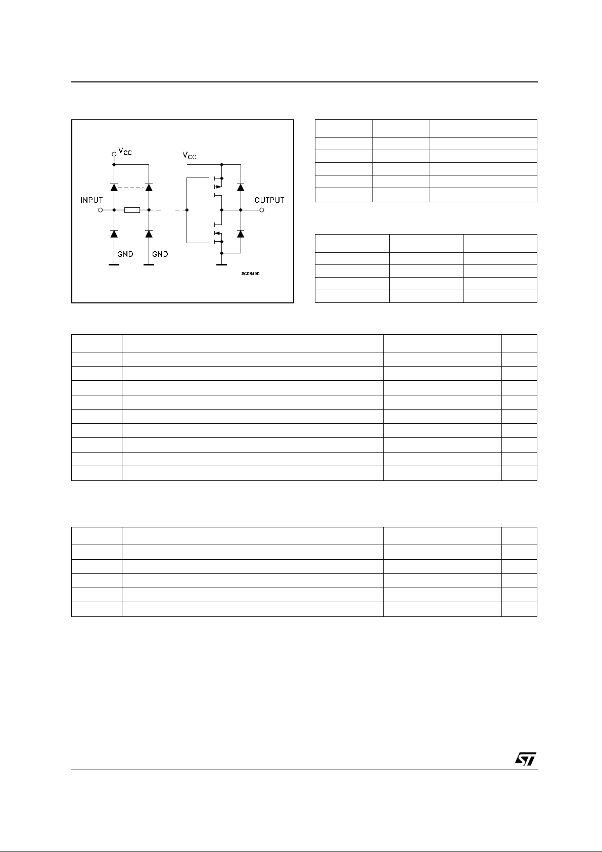
INPUT AND OUTPUT EQUIVALENT CIRCUIT PIN DESCRIPTION
PIN No SYMBOL NAME AND FUNCTION
1, 4, 9, 12 1A to 4A Data Inputs
2, 5, 10, 13 1B to 4B Data Inputs
3, 6, 8, 11 1Y to 4Y Data Outputs
7 GND Ground (0V)
14
V
CC
TRUTH TABLE
ABY
LLH
LHH
HLH
HHL
ABSOLUTE MAXIMUM RATINGS
Symbol Parameter Value Unit
V
V
V
I
I
OK
I
or I
I
CC
T
T
Absolute Maximum Ratings are those values beyond which damage to the device may occur. Functional operation under these conditions is
not implied.
Supply Voltage
CC
DC Input Voltage -0.5 to VCC + 0.5
I
DC Output Voltage -0.5 to VCC + 0.5
O
DC Input Diode Current
IK
DC Output Diode Current
DC Output Current
O
DC VCC or Ground Current
GND
Storage Temperature
stg
Lead Temperature (10 sec)
L
Positive Supply Voltage
-0.5 to +7 V
±
20 mA
±
20 mA
±
50 mA
±
200 mA
-65 to +150
300 °C
V
V
°C
RECOMMENDED OPERATING CONDITIONS
Symbol Parameter Value Unit
V
V
V
T
dt/dv
1) VIN from 0.8V to 2.0V
2/8
Supply Voltage
CC
Input Voltage 0 to V
I
Output Voltage 0 to V
O
Operating Temperature
op
Input Rise and Fall Time V
= 4.5 to 5.5V (note 1)
CC
4.5 to 5.5 V
CC
CC
-55 to 125 °C
8 ns/V
V
V
DC SPECIFICATIONS
Test Condition Value
T
Symbol Parameter
V
CC
(V)
V
V
V
V
I
CCT
I
I
OLD
I
OHD
1) Maxim um test duration 2ms, one output loaded at tim e
2) Incid ent wave switching is guaranteed on transmission l i nes with impe dances as low as 50Ω
High Level Input
IH
Voltage
Low Level Input
IL
Voltage
High Level Output
OH
Voltage
Low Level Output
OL
Voltage
I
Input Leakage Cur-
I
rent
Max ICC/Input
Quiescent Supply
CC
Current
Dynamic Output
Current (note 1, 2)
4.5 VO = 0.1 V or
V
-0.1V
CC
4.5 VO = 0.1 V or
V
5.5 1.5 0.8 0.8 0.8
4.5
5.5
4.5
5.5
4.5
5.5
4.5
5.5
V
5.5
5.5
V
5.5
V
5.5
V
-0.1V
CC
=-50 µA
I
O
I
=-50 µA
O
I
=-24 mA
O
I
=-24 mA
O
=50 µA
I
O
I
=50 µA
O
I
=24 mA
O
I
=24 mA
O
= VCC or GND
I
VI = VCC - 2.1V
= VCC or GND
I
= 1.65 V max
OLD
= 3.85 V min
OHD
= 25°C
A
Min. Typ. Max. Min. Max. Min. Max.
2.0 1.5 2.0 2.0
1.5 0.8 0.8 0.8
4.4 4.49 4.4 4.4
5.4 5.49 5.4 5.4
3.86 3.76 3.7
4.86 4.76 4.7
0.001 0.1 0.1 0.1
0.001 0.1 0.1 0.1
0.36 0.44 0.5
0.36 0.44 0.5
± 0.1 ± 1 ± 1 µA
0.6 1.5 1.6 mA
22040µ
74ACT00
-40 to 85°C -55 to 125°C
75 50
-75 -50
Unit
V5.5 2.0 1.5 2.0 2.0
V
V
A
mA
mA
AC ELECTRICAL CHARACTERISTICS (CL = 50 pF, RL = 500 Ω, Input tr = tf = 3ns)
Test Condition Value
T
Symbol Parameter
t
PLH tPHL
(*) Vol tage range is 5.0V ± 0.5V
Propagation Delay
Time
V
5.0
(V)
CC
= 25°C
A
Min. Typ. Max. Min. Max. Min. Max.
(*)
1.5 4.5 9.0 1.0 9.5 1.0 9.5 ns
-40 to 85°C -55 to 125°C
Unit
CAPACITIVE CHARACTERISTICS
Test Condition Value
= 25°C
Symbol Parameter
V
CC
(V)
C
C
1) CPD is defined as the value of the IC’s internal equivalent capacitance which is calculated from the operating current consumption without
load. (Refer to Test Circuit). Average operating current can be obtained by the following equation. I
Input Capacitance
IN
Power Dissipation
PD
Capacitance (note 1)5.0
5.0 4 pF
= 10MHz
f
IN
T
A
Min. Typ. Max. Min. Max. Min. Max.
31 pF
-40 to 85°C -55 to 125°C
= CPD x VCC x fIN + ICC/4 (per gate)
CC(opr)
Unit
3/8
 Loading...