

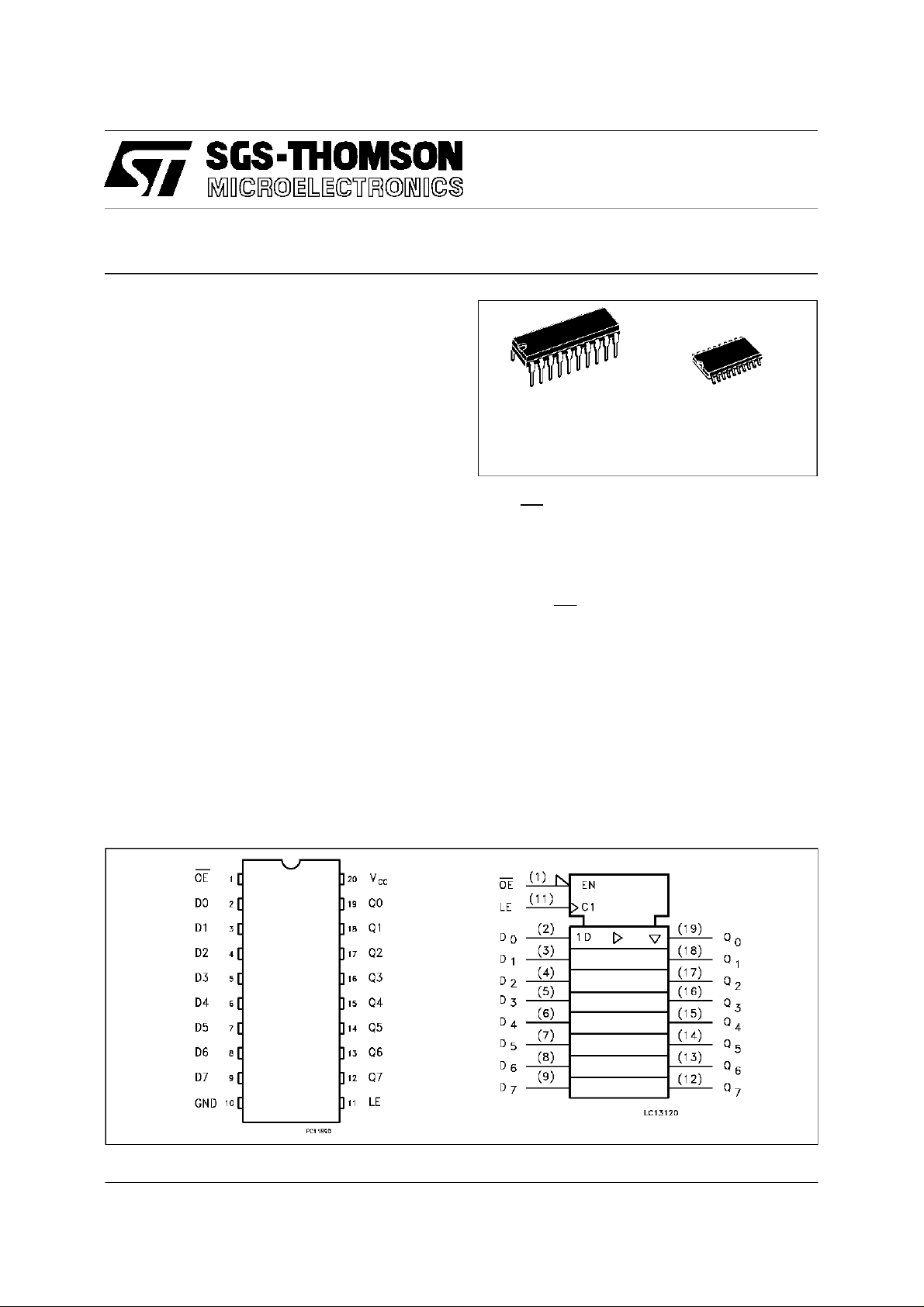
74AC573
OCTAL D-TYPE LATCH
WITH 3 STATE OUTPUT NON INVERTING
■ HIGH SPEED: t
■ LOWPOWER DISSIPATION:
=8µA (MAX.) at TA=25oC
I
CC
■ HIGH NOISE IMMUNITY:
V
NIH=VNIL
■ 50Ω TRANSMISSIONLINE DRIVING
= 4.5 ns(TYP.) at VCC=5V
PD
=28%VCC(MIN.)
CAPABILITY
■ SYMMETRICAL OUTPUT IMPEDANCE:
|I
|=IOL=24 mA (MIN)
OH
■ BALANCEDPROPAGATIONDELAY S:
t
≅ t
PLH
PHL
■ OPERATINGVOLTAGERAN GE:
V
(OPR) = 2V to 6V
CC
■ PIN AND FUNCTION COMPATIBLE WITH
74SERIES573
■ IMPROVED LATCH-UP IMMUNITY
DESCRIPTION
The AC573 is an advanced high-speed CMOS
OCTAL D-TYPE LATCH with 3 STATE OUTPUT
NON INVERTING fabricated with sub-micron
silicon gate and double-layermetal wiringC
2
MOS
technology. It is ideal for low power applications
mantaining high speed operation similar to
equivalentBipolarSchottkyTTL.
These 8 bit D-Type latches are controlled by a
B
(Plastic Package)
(Micro Package)
M
ORDERCODES:
74AC573B 74AC573M
latch enable input (LE) and an output enable
input (OE).
While the LE input is held at a high level, the Q
outputswill follow the data input precisely.
When the LE is taken low, the Q outputs will be
latchedpreciselyat thelogic level of D inputdata.
While the (OE) input is low, the 8 outputs will be
in a normal logic state (high or low logic level)
and while high level the outputs will be in a high
impedancestate.
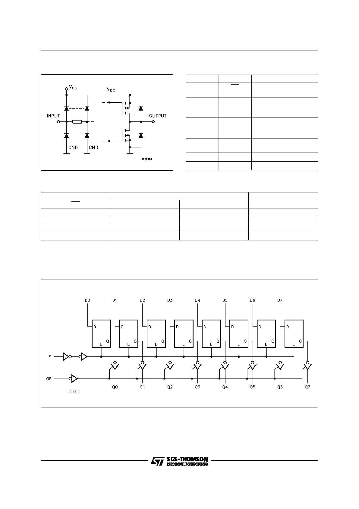
All inputs and outputs are equipped with
protectioncircuits against static discharge, giving
them 2KV ESD immunity and transient excess
voltage.
PINCONNECTION AND IEC LOGICSYMBOLS
April 1997
1/10
74AC573
INPUTAND OUTPUTEQUIVALENTCIRCUIT PIN DESCRIPTION
PI N No SYM B O L NAME AND F UNC T I ON
1 OE 3 State Output Enable
2, 3, 4,
5, 6, 7,
8, 9
12, 13, 14,
15, 16, 17,
18, 19
11 LE Latch Enable
10 GND Ground (0V)
20 V
TRUTH TABLE
INPUTS OUTPUTS
OE LE D Q
HXXZ
L L X NO CHANGE *
LHLL
LHHH
X:Don’tcare
Z: High impedance
* Q output are latched at the timewhen the LEinputs taken low logic level.
D0 to D7 Data Inputs
Q0 to Q7 3 State Latch Outputs
CC
Input (Active LOW)
Input
Positive Supply Voltage
LOGICDIAGRAM
2/10
74AC573
ABSOLUTE MAXIMUM RATINGS
Symb o l Parameter Val u e Uni t
V
V
V
I
I
OK
I
orI
I
CC
T
T
Absolute Maximum Ratings are those values beyond which damage to the device may occur. Functional operation under these condition is not implied.
RECOMMENDED OPERATINGCONDITIONS
Symb o l Parameter Value Un i t
V
V
V
T
dt/dv Input Rise and Fall Time V
1) VINfrom30%to70%of V
Supply Voltage -0.5 to +7 V
CC
DC Input Voltage -0.5 to VCC+ 0.5 V
I
DC Output Voltage -0.5 to VCC+ 0.5 V
O
DC Input Diode Current ± 20 mA
IK
DC Output Diode Current ± 20 mA
DC Output Current ± 50 mA
O
DC VCCor Ground Current ± 400 mA
GND
Storage Temperature -65 to +150
stg
Lead Temperature (10 sec) 300
L
Supply Voltage 2 to 6 V
CC
Input Voltage 0 to V
I
Output Voltage 0 to V
O
Operating Temperature: -40 to +85
op
= 3.0, 4.5 or 5.5 V(note 1) 8 ns/V
CC
CC
CC
CC
o
C
o
C
V
V
o
C
3/10
 Loading...