

SGS Thomson Microelectronics 74AC541 Datasheet
74AC541
OCTAL BUS BUFFER
WITH 3 STATE OUTPUTS (NON INVERTED)
■ HIGH SPEED:t
■
LOW POWERDISSIPATION:
I
=8 µA(MAX.) at TA=25oC
CC
■
HIGH NOISEIMMUNITY:
V
NIH=VNIL
■ 50Ω TRANSMISSIONLINEDRIVING
=28%VCC(MIN.)
=4ns(TYP.)atVCC=5V
PD
CAPABILITY
■ SYMMETRICAL OUTPUTIMPEDANCE:
|I
|=IOL=24 mA(MIN)
OH
■ BALANCEDPROPAGATIONDELAYS:
t
≅ t
PLH
PHL
■
OPERATINGVOLTAGERANGE:
V
(OPR)= 2Vto 6V
CC
■ PINANDFUNCTIONCOMPATIBLEWITH
74SERIES541
■ IMPROVEDLATCH-UP IMMUNITY
DESCRIPTION
The AC541 is an advanced CMOS OCTAL BUS
BUFFER (3-STATE) fabricated with sub-micron
silicon gate and double-layermetal wiring C
2
MOS
technology. It is ideal for low power applications
mantaining high speed operation similar to
B
(PlasticPackage)
(Micro Package)
M
ORDERCODES :
74AC541B 74AC541M
equivalentBipolarSchottky TTL.
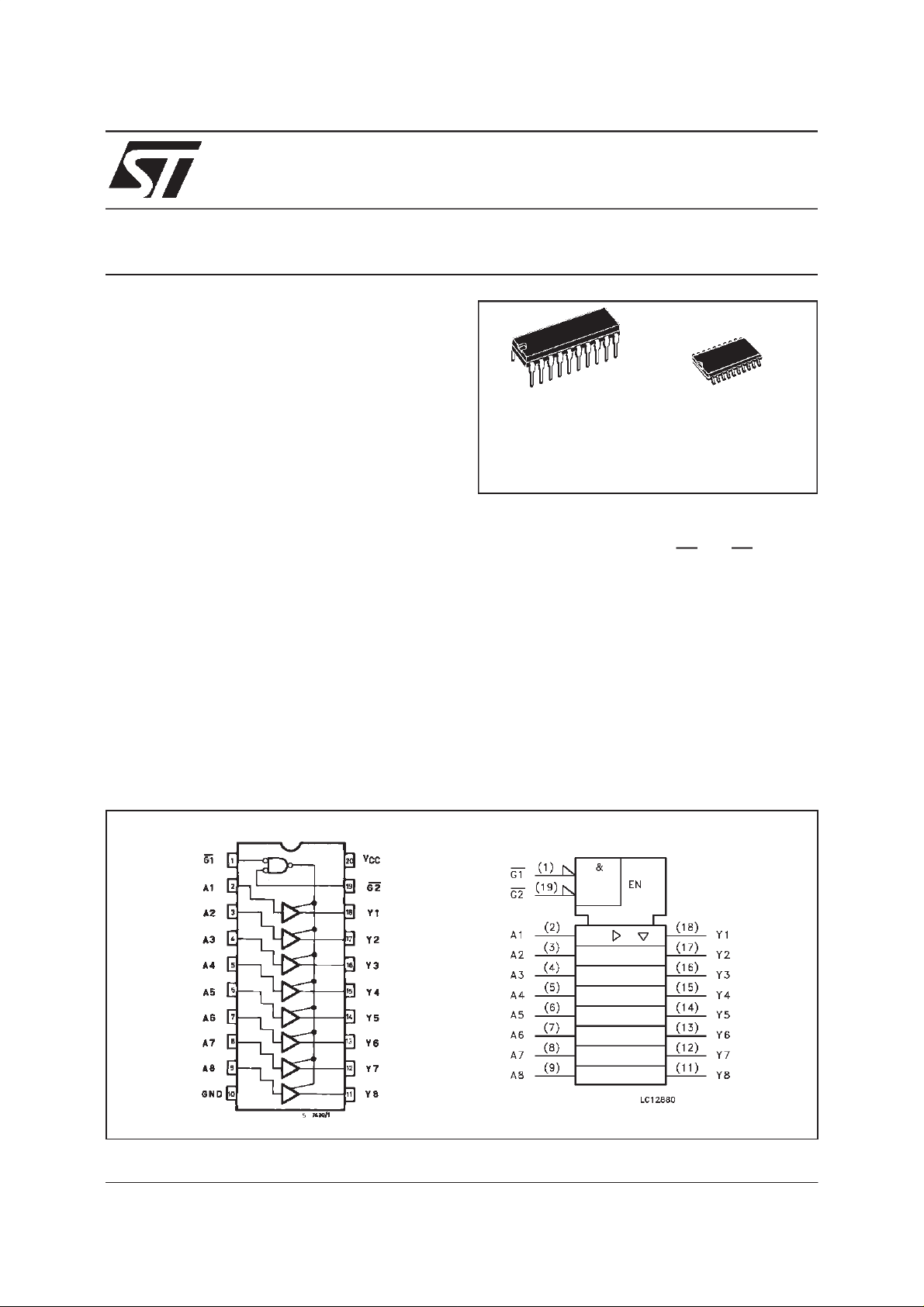
The 3 STATE control gate operates as a two
input AND such that if eitherG1 and G2 are high,
all eight outputs are in the high impedance state.
In order to enhance PC board layout, the AC541
offers a pinout having inputs and outputs on
opposite sidesof the package.
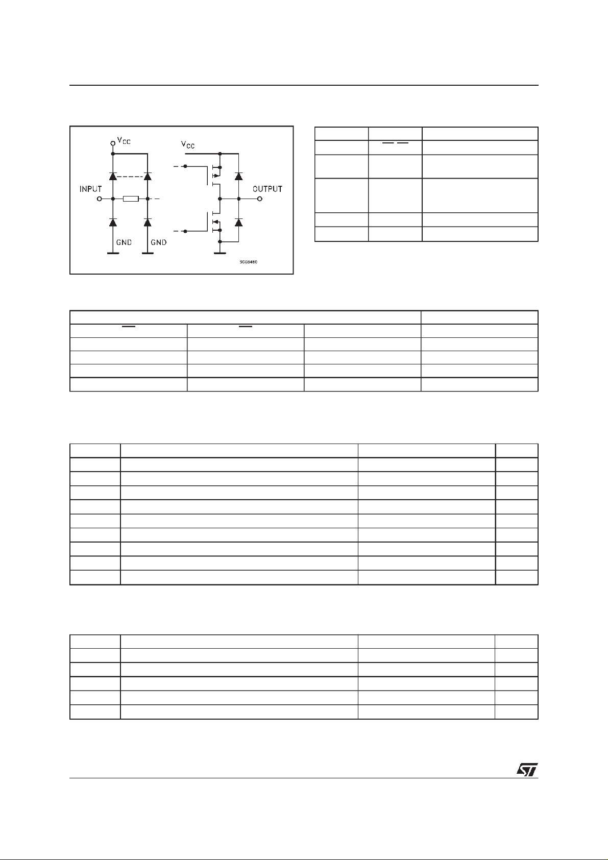
All inputs and outputs are equipped with
protection circuits against static discharge, giving
them 2KV ESD immunity and transient excess
voltage.
PIN CONNECTION AND IEC LOGIC SYMBOLS
November 1998
1/8
74AC541
INPUT AND OUTPUT EQUIVALENT CIRCUIT
TRUTH TABLE
INPUT OUTPUT
G1 G2 An Yn
HXXZ
XHXZ
LLHH
LLLL
X:”H” or”L”
Z:Highimpedance
PIN DESCRIPTION
PI N No SYM BO L NAM E AND F U NCTIO N
1,19 G1,G2 Output Enable Input
2,3,4,5,
6,7,8,9
18,17,16,
15,14,13,
12, 11
10 GND Ground (0V)
20 V
A1toA8 Data Inputs
Y1toY8 Data Outputs
Positive Supply Voltage
CC
ABSOLUTE MAXIMUM RATINGS
Symb o l P ara met er Val u e Uni t
V
V
V
I
I
OK
I
orI
I
CC
T
T
AbsoluteMaximumRatingsarethosevalues beyondwhichdamagetothedevicemayoccur.Functionaloperationunderthese condition isnotimplied.
Supply Voltage -0.5to+7 V
CC
DC Input Voltage -0.5toVCC+0.5 V
I
DC Output Voltage -0.5toVCC+0.5 V
O
DC Input Diode Current
IK
DC Output Diode Current
DC Output Current ±50 mA
O
DC VCCor Ground Current ±400 mA
GND
Storage Temperature -65to+150
stg
Lead Temperature (10 sec) 300
L
20 mA
±
20 mA
±
o
C
o
C
RECOMMENDED OPERATINGCONDITIONS
Symb o l P ara met er Value Un it
V
V
V
T
dt/dv Input Rise and Fall Time V
1)VINfrom30%to70%of V
Supply Voltage 2to6 V
CC
Input Voltage 0toV
I
Output Voltage 0toV
O
Operating Temperature: -40to+85
op
= 3.0, 4.5 or 5.5 V(note 1) 8 ns/V
CC
CC
CC
CC
V
V
o
C
2/8
74AC541
DC SPECIFICATIONS
Symbol Parameter Test Conditions Value Unit
T
V
CC
(V)
High Level Input Voltage 3.0 VO=0.1V or
V
IH
4.5 3.15 2.25 3.15
V
CC
-0.1V
5.5 3.85 2.75 3.85
Low Level Input Voltage 3.0 VO=0.1V or
V
IL
4.5 2.25 1.35 1.35
V
CC
-0.1V
5.5 2.75 1.65 1.65
High Level Output
V
OH
Voltage
Low Level Output
V
OL
Voltage
Input Leakage Current 5.5 VI=VCCorGND ±0.1 ±1 µA
I
I
3 State Output Leakage
I
OZ
Current
Quiescent Supply
I
CC
3.0
4.5 I
5.5 I
3.0 I
V
I
V
IH
V
4.5 I
5.5 I
3.0
4.5 I
5.5 I
3.0 I
V
I
V
IH
V
4.5 I
5.5 I
5.5 VI=VIHorV
IO=-50µA 2.9 2.99 2.9
(*)
or
IL
=-50µA 4.4 4.49 4.4
O
=
=-50µA 5.4 5.49 5.4
O
=-12 mA 2.56 2.46
O
=-24 mA 3.86 3.76
O
=-24 mA 4.86 4.76
O
IO=50µA 0.002 0.1 0.1
(*)
=
or
IL
=50µA 0.001 0.1 0.1
O
=50
µΑ
O
=12mA 0.36 0.44
O
=24mA 0.36 0.44
O
=24mA 0.36 0.44
O
IL
VO=VCCorGND
5.5 VI=VCCorGND 8 80 µA
Current
Dynamic Output Current
I
OLD
(note 1, 2)
I
OHD
1) Maximum testduration 2ms,one output loaded attime
2)Incidentwaveswitchingisguaranteed ontransmissionlineswithimpedances aslowas50 Ω.
(*)All outputs loaded.
5.5 V
=1.65V max 75 mA
OLD
V
=3.85V min -75 mA
OHD
=25oC -40 to 85oC
A
Min. Typ. Max. Min. Max.
2.1 1.5 2.1
1.5 0.9 0.9
0.001 0.1 0.1
0.5
±
5
±
µ
V
V
V
V
A
3/8
 Loading...