

WITH 3 STATE OUTPUT NON INVERTING
■ HIGH SPEED:
■ f
■ LOWPOWER DISSIPATION:
■ HIGH NOISE IMMUNITY:
■ 50Ω TRANSMISSION LINE DRIVING
■ SYMMETRICAL OUTPUT IMPEDANCE:
■ BALANCEDPROPAGATIONDELAY S:
■ OPERATINGVOLTAGERAN GE:
■ PIN AND FUNCTION COMPATIBLE WITH
■ IMPROVED LATCH-UP IMMUNITY
DESCRIPTION
The AC374 is an advanced high-speed CMOS
OCTAL D-TYPE FLIP FLOP with 3 STATE
OUTPUT NON INVERTING fabricated with
sub-micron silicon gate and double-layer metal
wiring C
power applications mantaining high speed
operation similar to equivalent Bipolar Schottky
TTL.
These 8 bit D-Type flip-flops are controlled by a
= 270 MHz (TYP.)at VCC=5V
MAX
=8µA (MAX.) at TA=25oC
I
CC
V
NIH=VNIL
=28%VCC(MIN.)
CAPABILITY
|I
|=IOL=24 mA (MIN)
OH
≅ t
t
PLH
PHL
V
(OPR) = 2V to 6V
CC
74SERIES374
2
MOS technology. It is ideal for low
74AC374
OCTAL D-TYPE FLIP FLOP
B
(Plastic Package)
(Micro Package)
ORDERCODES:
74AC374B 74AC374M
clockinput (CK)and an output enable input(OE).
On the positive transition of the clock, the Q
outputs will be set to the logic state that were
setupat the D inputs.
While the (OE) input is low, the 8 outputs will be
in a normal logic state (high or low logic level)
and while high level the outputs will be in a high
impedancestate.
The output control does not affect the internal
operation of flip flops; that is, the old data can be
retained or the new data can be entered even
while the outputsare off.
All inputs and outputs are equipped with
protectioncircuits against static discharge, giving
them 2KV ESD immunity and transient excess
voltage.
M
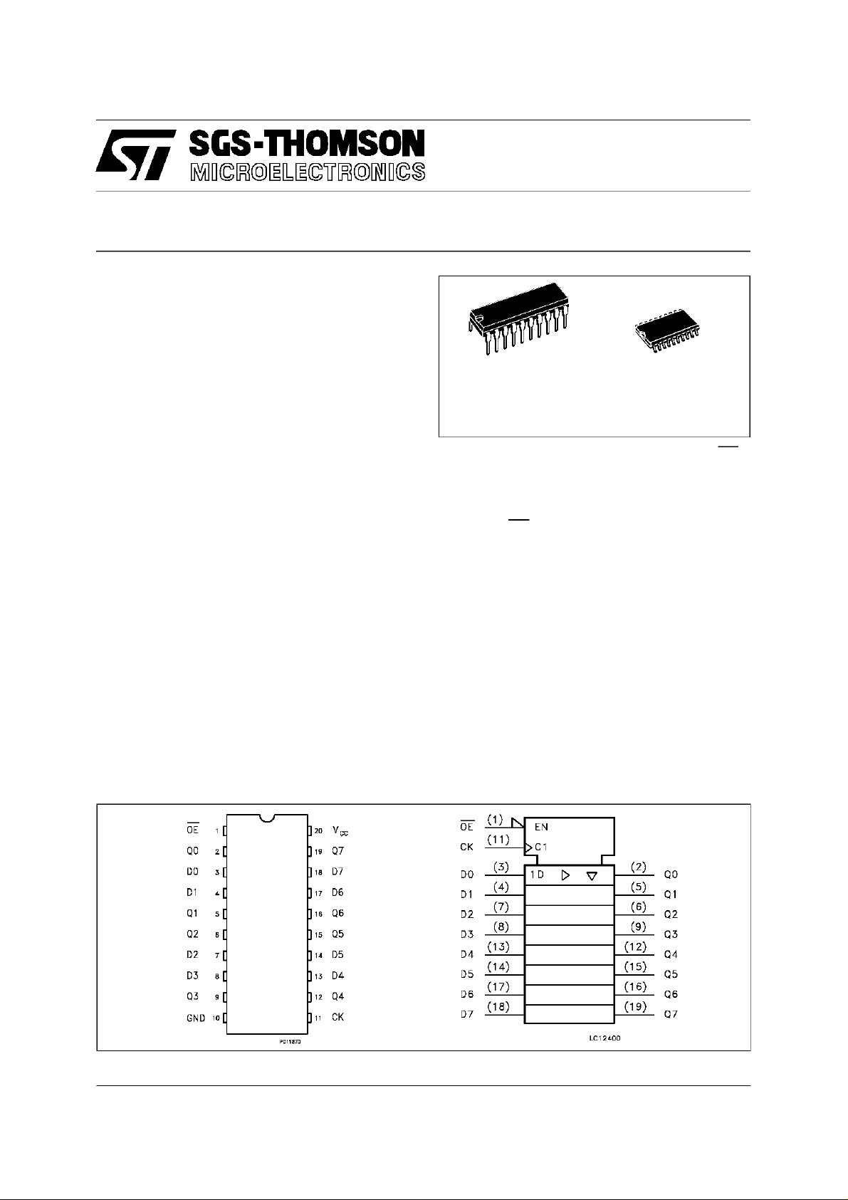
PINCONNECTION AND IEC LOGIC SYMBOLS
April 1997
1/10
74AC374
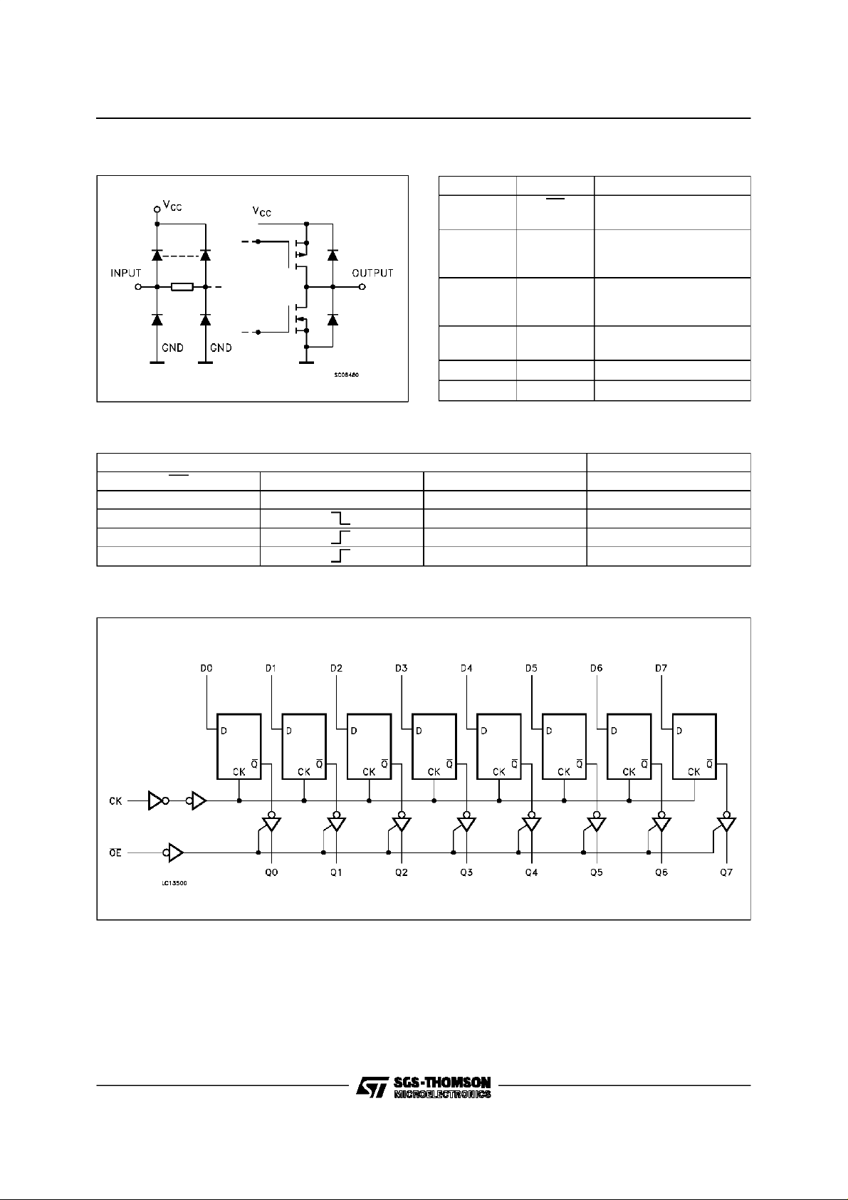
INPUTAND OUTPUTEQUIVALENTCIRCUIT PIN DESCRIPTION
PI N No SYM B O L NAME AND FUNCT I ON
1 OE 3 State Output Enable
2, 5, 6, 9,
12, 15, 16,
19
3, 4, 7, 8,
13, 14, 17,
18
11 CLOCK Clock Input (LOW to
10 GND Ground (0V)
20 V
TRUTH TABLE
INPUTS OUTPUTS
OE CK D Q
HXXZ
L X NO CHANGE
LLL
LHH
Q0 to Q7 3 State Outputs
D0 to D7 Data Inputs
CC
Input (Active LOW)
HIGH, edge triggered)
Positive Supply Voltage
LOGICDIAGRAM
2/10
74AC374
ABSOLUTE MAXIMUM RATINGS
Symb o l Parame t er Val u e Uni t
V
V
V
I
I
OK
I
orI
I
CC
T
T
Absolute Maximum Ratings are those values beyond which damage to the device may occur. Functional operation under these condition isnot implied.
RECOMMENDED OPERATINGCONDITIONS
Symb o l Parame t er Value Un i t
V
V
V
T
dt/dv Input Rise and Fall Time V
1) VINfrom30%to70%of V
Supply Voltage -0.5 to +7 V
CC
DC Input Voltage -0.5 to VCC+ 0.5 V
I
DC Output Voltage -0.5 to VCC+ 0.5 V
O
DC Input Diode Current ± 20 mA
IK
DC Output Diode Current ± 20 mA
DC Output Current ± 50 mA
O
DC VCCor Ground Current ± 400 mA
GND
Storage Temperature -65 to +150
stg
Lead Temperature (10 sec) 300
L
Supply Voltage 2 to 6 V
CC
Input Voltage 0 to V
I
Output Voltage 0 to V
O
Operating Temperature: -40 to +85
op
= 3.0, 4.5 or 5.5 V(note 1) 8 ns/V
CC
CC
CC
CC
o
C
o
C
V
V
o
C
3/10
 Loading...