

HEX D-TYPE FLIP FLOP WITH CLEAR
■ HIGH SPEED:
=125MHz (TYP.)at VCC=5V
f
MAX
■ LOWPOWER DISSIPATION:
=8µA (MAX.) at TA=25oC
I
CC
■ HIGH NOISE IMMUNITY:
V
NIH=VNIL
■ 50Ω TRANSMISSION LINE DRIVING
CAPABILITY
■ SYMMETRICAL OUTPUT IMPEDANCE:
|I
|=IOL=24 mA (MIN)
OH
■ BALANCEDPROPAGATIONDELAY S:
≅ t
t
PLH
■ OPERATINGVOLTAGERAN GE:
V
CC
■ PIN AND FUNCTION COMPATIBLEWITH
74SERIES174
■ IMPROVED LATCH-UP IMMUNITY
DESCRIPTION
The AC174 is an high-speed CMOS HEX
D-TYPE FLIP FLOP WITH CLEAR fabricated
with sub-micron silicon gate and double-layer
metal wiring C
power applications mantaining high speed
operation similar to eqivalent Bipolar Schottky
=28%VCC(MIN.)
PHL
(OPR) = 2V to 6V
2
MOS technology. It is ideal for low
74AC174
PRELIMINARY DATA
B
(Plastic Package)
(Micro Package)
ORDERCODES:
74AC174B 74AC174M
TTL.
Information signals applied to D inputs are
transfered to the Q output on the positive going
edgeof the clockpulse.
Whenthe CLEARinput is held low, the Q outputs
are held low independentelyof the other inputs .
All inputs and outputs are equipped with
protectioncircuits againststatic discharge, giving
them 2KV ESD immunity and transient excess
voltage.
M
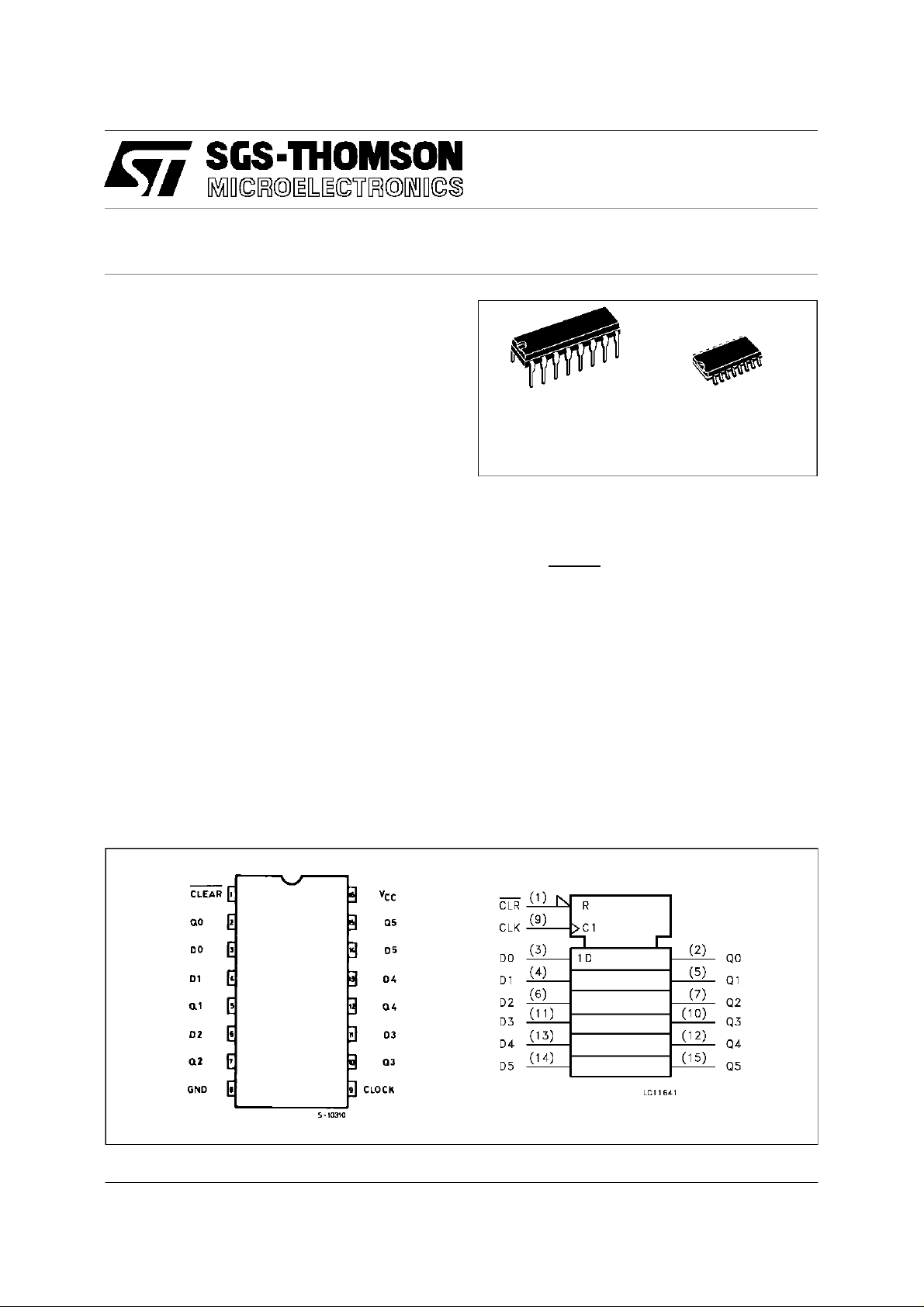
PINCONNECTION AND IEC LOGIC SYMBOLS
May 1997
1/10
74AC174
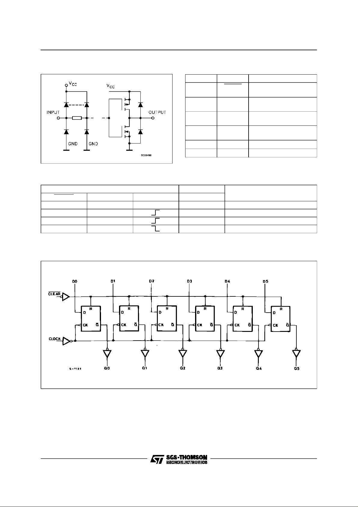
INPUTAND OUTPUTEQUIVALENTCIRCUIT
TRUTH TABLE
INP UT S OUT PUTS FUNCT ION
CLEAR D CLOCK Q
L X X L CLEAR
HL L
HH H
HX Q
X:Don’tCare
PIN DESCRIPTION
PI N No SYM B O L NAME AND FUNC T I ON
1 CLEAR Asyncronous Master Reset
(ActiveLOW)
2, 5, 7, 10,
12, 15
3, 4, 6, 11,
13, 14
9 CLOCK Clock Input(LOW-to-HIGH,
8 GND Ground (0V)
16 V
n
Q0 to Q5 Flip-Flop Outpus
D0 to D5 DataInputs
Edge-Triggered)
CC
PositiveSupply Voltage
NO CHANGE
LOGICDIAGRAM
This logic diagram has not be used to estimate propagation delays
2/10
74AC174
ABSOLUTE MAXIMUM RATINGS
Symb o l Parame t er Val u e Uni t
V
V
V
I
I
OK
I
orI
I
CC
T
T
Absolute Maximum Ratings are those values beyond which damage to the device may occur. Functional operation under these condition is not implied.
RECOMMENDED OPERATINGCONDITIONS
Symb o l Parame t er Value Un i t
V
V
V
T
dt/dv Input Rise and FallTimeV
1) VINfrom30%to70%of V
Supply Voltage -0.5 to +7 V
CC
DC Input Voltage -0.5 to VCC+ 0.5 V
I
DC OutputVoltage -0.5 to VCC+ 0.5 V
O
DC Input Diode Current ± 20 mA
IK
DC OutputDiodeCurrent ± 20 mA
DC OutputCurrent ± 50 mA
O
DC VCCorGround Current ± 300 mA
GND
Storage Temperature -65 to +150
stg
LeadTemperature (10 sec) 300
L
Supply Voltage 2 to 6 V
CC
Input Voltage 0 to V
I
OutputVoltage 0 to V
O
Operating Temperature: -40 to +85
op
=3.0,4.5 or 5.5 V(note1) 8 ns/V
CC
CC
CC
CC
o
C
o
C
V
V
o
C
3/10
 Loading...