

1/10February 2003
■ HIGH SPEED:
t
PD
= 5.0 ns (TYP.) at VCC=5V
■ LOW POWER DISSIPATION:
I
CC
=8µA(MAX.) at TA=25°C
■ HIGH NOISE IMMUNITY:
V
NIH=VNIL
=28%VCC(MIN.)
■ 50ΩTRASMISSION LINE DRIVING
CAPABILITY
■ SYMMETRICAL OUTPUT IMPEDANCE:
|I
OH
|=IOL= 24mA (MIN)
■ OPERATING VOLTAGE RANGE:
V
CC
(OPR) = 2V to 6V
■ IMPROVED LATCH-UP IMMUNITY
DESCRIPTION
The 74AC16373 CMOS 16 BIT D-TYPE LATCH
with 3 STATE OUTPUTS NON INVERTING
fabricated with sub-micron silicon gate and
double-layer metal wiring C
2
MOS technology.
These 16 bit D-TYPE latches are byte controlled
by two latch enable inputs (nLE) and two output
enable inputs(nOE
).
While the nLE input is held at a high level, the nQ
outputs will follow the data (D) i nput s .
When the nLE is t ak en L OW, the nQ outputs will
be latched at the logic level of D data inputs.
When the (nOE
) input is low, the nQ outputs will
be in a normal lo gic s tate (high or low logic level);
when nOE
is at high level ,the outputs will be in a
high impedance state.
All inputs and outputs are equipped with
protection circuits against static discharge, giving
them 2KV ESD immunity and transient exc es s
voltage.
74AC16373
16-BIT D-TYPE FLIP-FLOP
WITH 3-STATE OUTPUTS (NON INVERTED)
ORDER CODES
PACKAGE TUBE T & R
TSSOP 74AC16373TTR
TSSOP
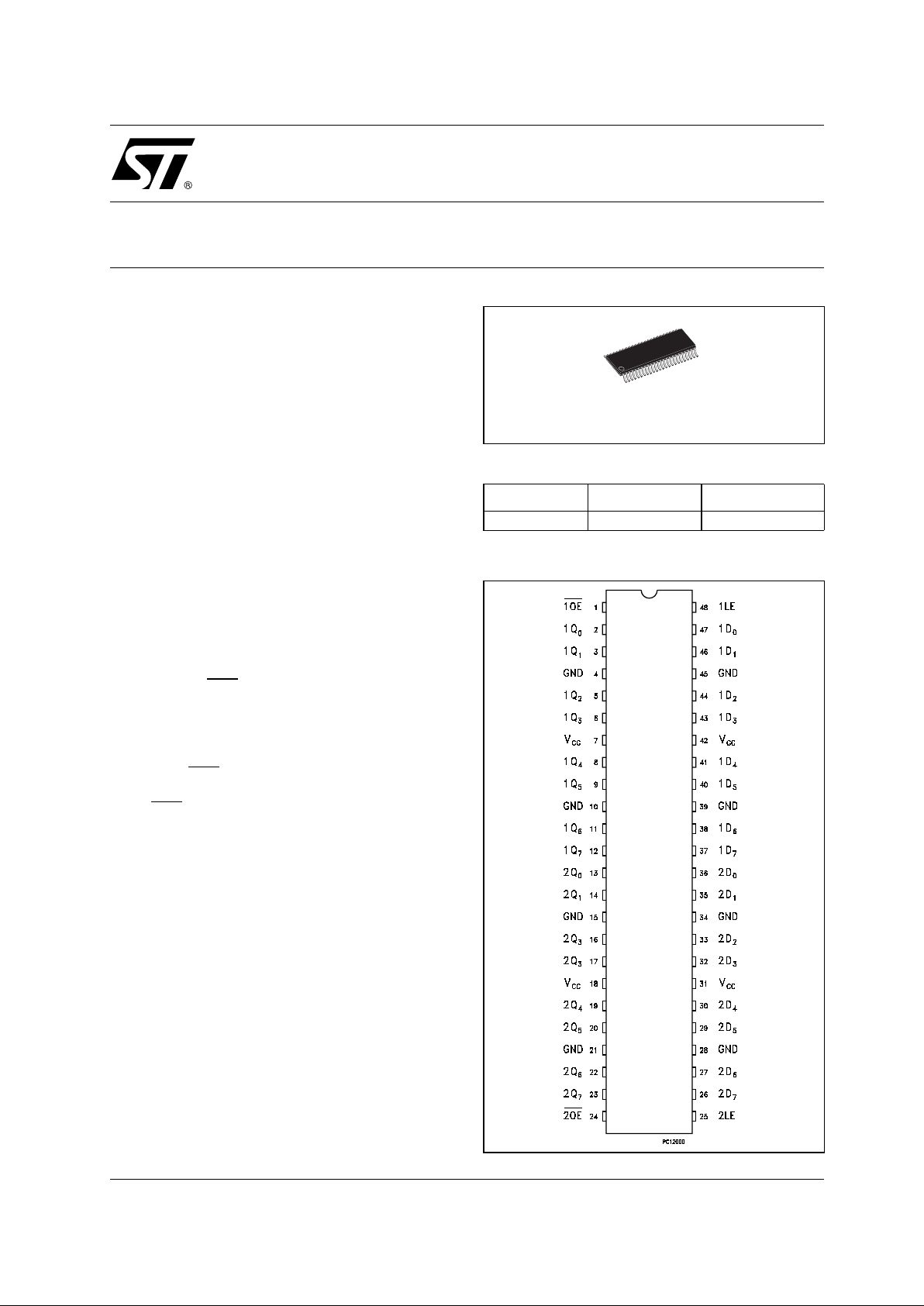
PIN CONNECTION
74AC16373
2/10
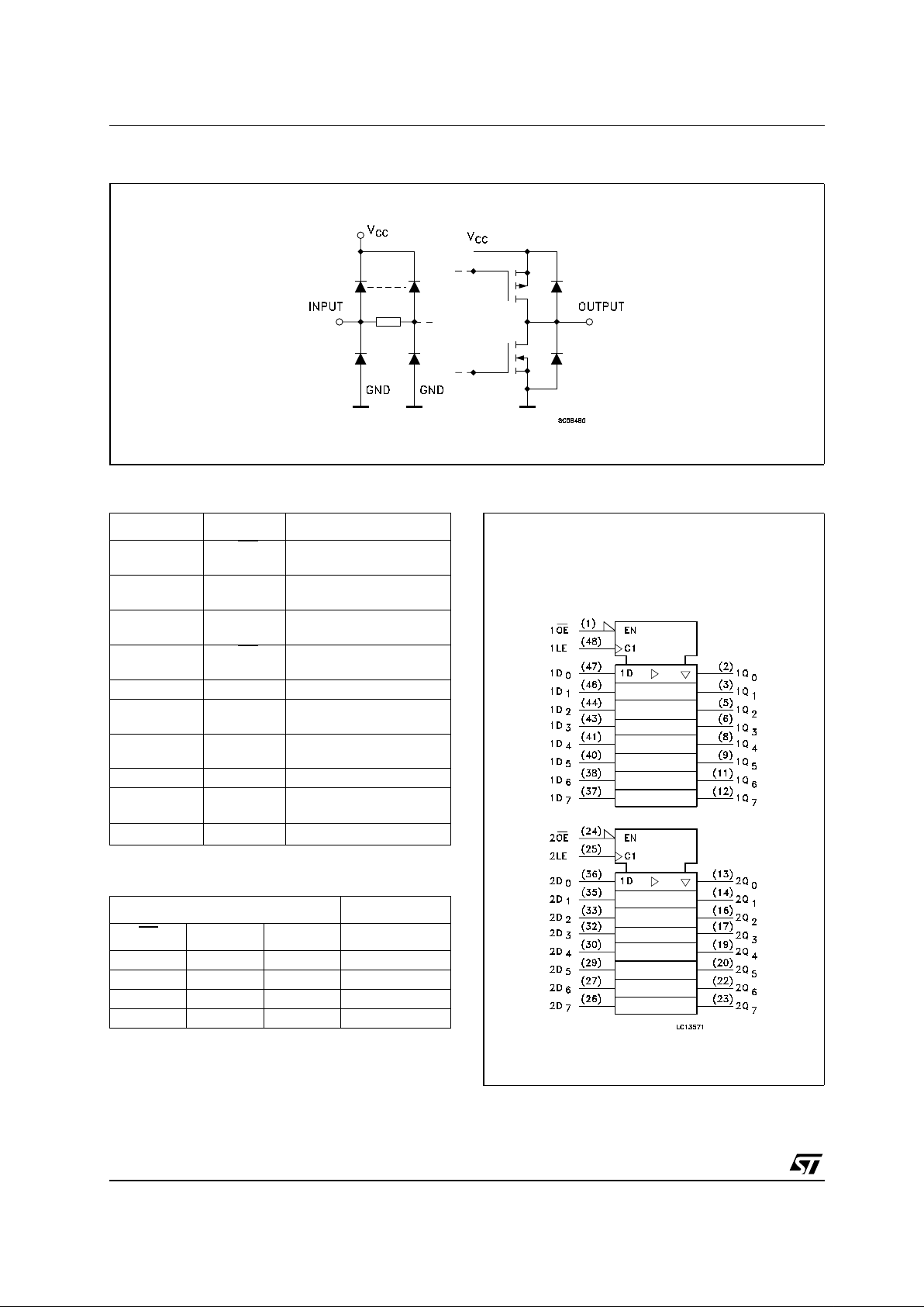
INPUT AND O UTPUT EQUIVALENT CIRCUIT
PIN DESCRIPTION
TRUTH TABLE
X : Don‘tCare
Z : High Impedance
* : Q outputs are latched at the time when the LEinputistaken low
logiclevel.
IEC L OGIC SYMBOLS
PIN No SYMBOL NAME AND FUNCTION
1 1OE
3 State Output Enable
Input (Active LOW)
2, 3, 5, 6, 8, 9,
11, 12
1Q0 to 1Q7 3-State Outputs
13,14,16,17,
19, 20, 22, 23
2Q0 to 2Q7 3-State Outputs
24 2OE
3 State Output Enable
Input (Active LOW)
25 2LE Latch Enable Input
36,35,33,32,
30, 29, 27, 26
2D0 to 2D7 Data Inputs
47,46,44,43,
41, 40, 38, 37
1D0 to 1D7 Data Inputs
48 1LE Latch Enable Input
4, 10, 15, 21,
28, 34, 39, 45
GND Ground (0V)
7, 18, 31, 42 V
CC
Positive Supply Voltage
INPUTS OUTPUT
OE
LE D Q
HXX Z
L L X NO CHANGE *
LHL L
LHH H
74AC16373
3/10
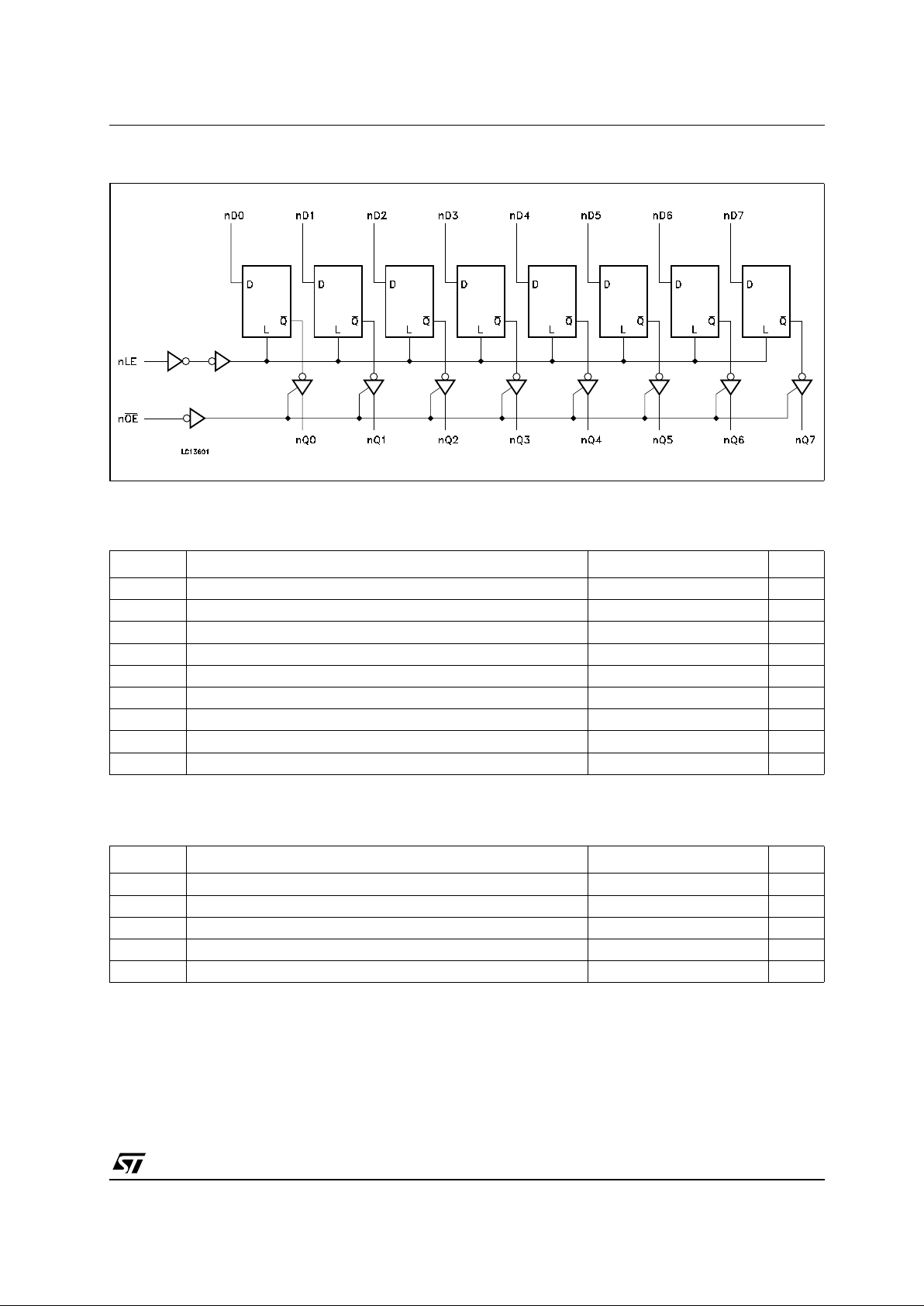
LOGIC DIAGRAM
This logic diagram has not to be used to estimate propagation delays
ABSOLUTE MAXIMUM RATINGS
Absolute Maximum Ratings are those values beyond which damage to the device may occur. Functional operation under these conditions is
not implied.
RECOMMENDED OPERATING CONDITIONS
1) VINfrom30% to 70% of V
CC
Symbol Parameter Value Unit
V
CC
Supply Voltage
-0.5 to +7 V
V
I
DC Input Voltage -0.5 to VCC+ 0.5
V
V
O
DC Output Voltage -0.5 to VCC+ 0.5
V
I
IK
DC Input Diode Current
± 20 mA
I
OK
DC Output Diode Current
± 20 mA
I
O
DC Output Current
± 50 mA
I
CC
or I
GND
DC VCCor Ground Current
± 400 mA
T
stg
Storage Temperature
-65 to +150 °C
T
L
Lead Temperature (10 sec)
300 °C
Symbol Parameter Value Unit
V
CC
Supply Voltage
2to6 V
V
I
Input Voltage 0 to V
CC
V
V
O
Output Voltage 0 to V
CC
V
T
op
Operating Temperature
-55 to 125 °C
dt/dv
Input Rise and Fall Time V
CC
= 3.0, 4.5 or 5.5V (note 1)
8 ns/V
 Loading...