

SGS Thomson Microelectronics 74AC161 Datasheet
SYNCHRONOUS PRESETTABLE 4-BIT COUNTER
■ HIGHSPEED:
f
=125MHz(TYP.)at VCC=5V
MAX
■ LOW POWER DISSIPATION:
=8 µA (MAX.) at TA=25oC
I
CC
■ HIGHNOISEIMMUNITY:
V
NIH=VNIL
■ 50Ω TRANSMISSIONLINEDRIVING
CAPABILITY
■ SYMMETRICALOUTPUTIMPEDANCE:
|I
|=IOL=24mA(MIN)
OH
■ BALANCEDPROPAGATIONDELAYS:
t
≅ t
PLH
■ OPERATINGVOLTAGERANGE:
V
(OPR)= 2Vto 6V
CC
■ PINANDFUNCTIONCOMPATIBLEWITH
74SERIES161
■ IMPROVEDLATCH-UPIMMUNITY
DESCRIPTION
The AC161 is a high-speed CMOS
SYNCRONOUS PRESETTABLE COUNTER
fabricated with sub-micron silicon gate and
double-layermetal wiring C
ideal for low power applications mantaining high
speed operation similar to eqivalent Bipolar
Schottky TTL. It is a 4 bit binary counter with
AsynchronousClear.
The circuit have four fundamental modes of
operation, in order of preference: synchronous
=28%VCC(MIN.)
PHL
2
MOS technology.It is
74AC161
B
(PlasticPackage)
(Micro Package)
ORDERCODES :
74AC161B 74AC161M
reset, parallel load, count-up and hold. Four
control inputs, Master Reset (CLEAR), Parallel
Enable Input (LOAD), Count Enable Input (PE)
and Count Enable Carry Input (TE), determine
the mode of operation as shown in the Truth
Table. A LOW signal on CLEAR overrides
counting and parallel loading and sets all outputs
on LOW state. A LOW signal on LOAD overrides
counting and allows information on Parallel Data
Qn inputs to be loaded into the flip-flops on the
next rising edge of CLOCK. With LOAD and
CLEAR, PE and TE permit counting when both
are HIGH. Conversely, a LOW signal on either
PE and TE inhibitscounting.
All inputs and outputs are equipped with
protection circuits against static discharge, giving
them 2KV ESD immunity and transient excess
voltage.
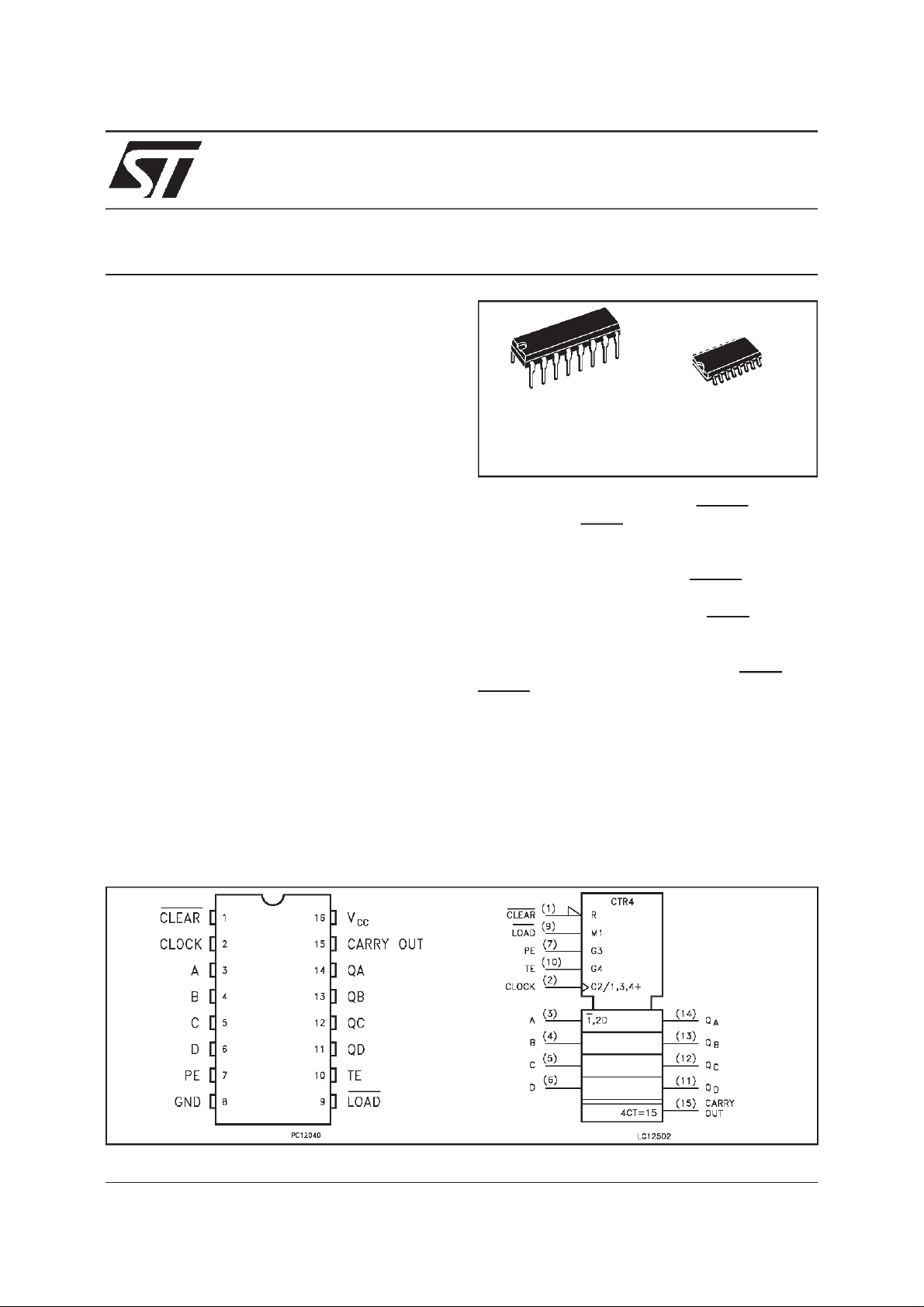
M
PIN CONNECTION AND IECLOGIC SYMBOLS
December 1998
1/12
74AC161
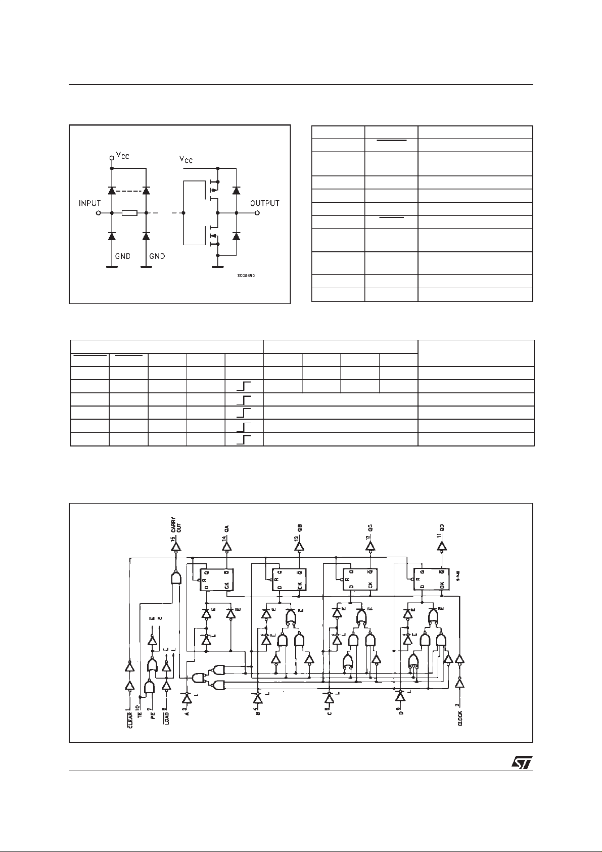
INPUT AND OUTPUTEQUIVALENTCIRCUIT
PIN DESCRIPTION
PI N No SYM BO L NAM E AND FU NCTION
1 CLEAR MasterReset
2 CLOCK ClockInput(LOW-to-HIGH,
Edge-Triggered)
3, 4, 5, 6 A, B, C, D Data Inputs
7 PE CountEnable Input
10 TE CountEnable CarryInput
9 LOAD ParallelEnableInput
14, 13,12,11QA to QD Flip-Flop Outpus
15 CARRY
OUT
8 GND Ground(0V)
16 V
CC
Terminal CountOutput
PositiveSupply Voltage
TRUTH TABLE
INPUTS OUTPUTS FUNCTION
CLEAR LOAD PE TE CLOCK QA QB QC QD
LXXXXLLLL RESET TO ”0”
H L X X A B C D PRESET DATA
H H X L NO CHANGE NO COUNT
H H L X NO CHANGE NO COUNT
H H H H COUNT UP COUNT
H X X X NO CHANGE NO COUNT
NOTE: X:Don’tCare
A,B, C,D: Logiclevelofdatainput
CARRYOUT=TE• QA• QB • QC • QD
LOGICDIAGRAMS
2/12
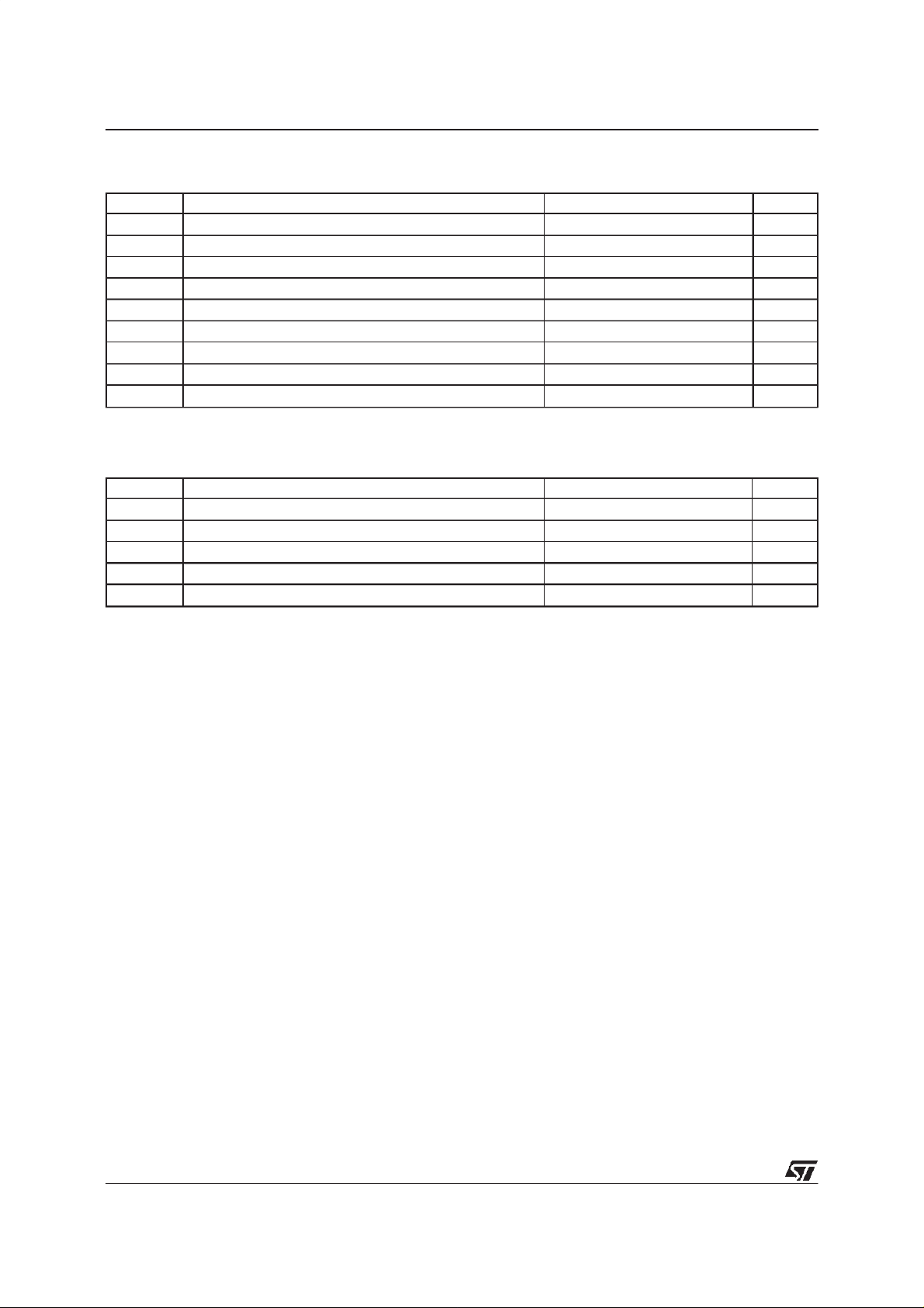
TIMINGCHART
74AC161
3/12
74AC161
ABSOLUTE MAXIMUM RATINGS
Symb o l Para met er Val u e Uni t
V
V
V
I
I
OK
I
or I
I
CC
T
T
AbsoluteMaximumRatingsarethosevaluesbeyond whichdamage tothedevice mayoccur.Functionaloperation underthesecondition isnotimplied.
RECOMMENDEDOPERATINGCONDITIONS
Symb o l Para met er Value Un it
V
V
V
T
dt/dv InputRiseand FallTime V
1)VINfrom30%to70%ofV
SupplyVoltage -0.5 to +7 V
CC
DC InputVoltage -0.5 to VCC+ 0.5 V
I
DC OutputVoltage -0.5 to VCC+ 0.5 V
O
DC InputDiode Current ± 20 mA
IK
DC OutputDiode Current ± 20 mA
DC OutputCurrent
O
DC VCCorGround Current
GND
Storage Temperature -65 to +150
stg
LeadTemperature (10 sec) 300
L
SupplyVoltage 2 to 6 V
CC
InputVoltage 0 to V
I
OutputVoltage 0 to V
O
OperatingTemperature: -40 to +85
op
=3.0,4.5 or 5.5V(note1) 8 ns/V
CC
CC
50 mA
±
300 mA
±
CC
CC
o
C
o
C
V
V
o
C
4/12
 Loading...