74AC14
HEX INVERTER
■ HIGH SPEED: t
■ LOWPOWERDISSIPATION:
I
=4µA (MAX.) at TA=25oC
CC
■ HIGH NOISE IMMUNITY:
V
NIH=VNIL
■ 50Ω TRANSMISSIONLINE DRIVING
=6 ns(TYP.)atVCC=3.3V
PD
=28%VCC(MIN.)
CAPABILITY
■ SYMMETRICAL OUTPUT IMPEDANCE:
|=IOL=24mA (MIN)
|I
OH
■ BALANCEDPROPAGAT IOND ELAY S:
t
≅ t
PLH
PHL
■ OPERATINGVOLTAGER ANGE:
V
(OPR) = 2V to 6V
CC
■ PIN AND FUNCTION COMPATIBLE WITH
74SERIES14
■ IMPROVED LATCH-UP IMMUNITY
DESCRIPTION
The AC14 is an advanced high-speed CMOS
HEX INVERTER fabricated with sub-micron
silicon gateand double-layermetal wiring C
2
MOS
technology. It is ideal for low power applications
mantaining high speed operation similar to
B
(Plastic Package)
(Micro Package)
M
ORDERCODES :
74AC14B 74AC14M
equivalentBipolarShottky TTL.
The internal circuit is composed of 3 stages
including buffer output, which enables high noise
immunityand stable output.
This together with its schmitt trigger function
allows it to be used on line receivers with slow
rise/fallinputsegnals.
All inputs and outputs are equipped with
protectioncircuits against static discharge, giving
them 2KV ESD immunity and transient excess
voltage.
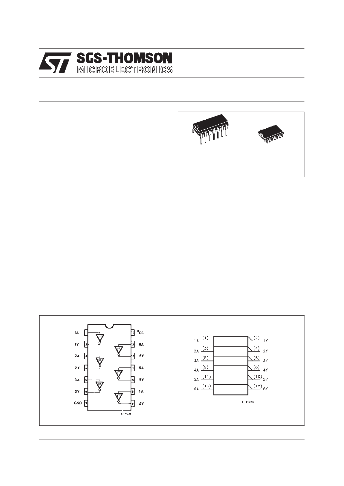
PINCONNECTION ANDIEC LOGIC SYMBOLS
March 1998
1/7

74AC14
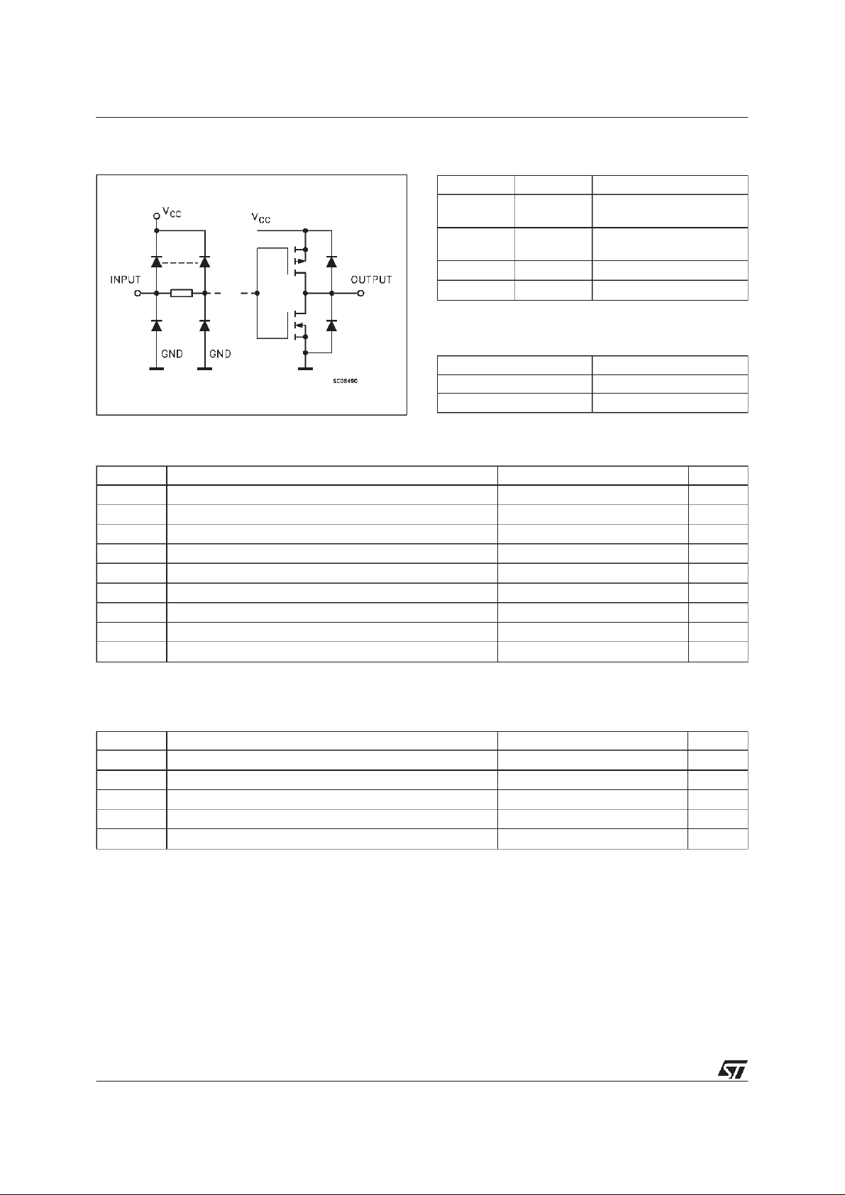
INPUTAND OUTPUT EQUIVALENTCIRCUIT
PIN DESCRIPTION
PI N No SYM B O L NAME AND F UNC T I ON
1, 3, 5, 9,
1A to 6A Data Inputs
11, 13
2, 4, 6, 8,
1Y to 6Y Data Oututs
10, 12
7 GND Ground (0V)
14 V
CC
Positive Supply Voltage
TRUTHTABLE
AY
LH
HL
ABSOLUTE MAXIMUM RATINGS
Symb o l Parame t er Val u e Uni t
V
V
V
I
I
OK
I
orI
I
CC
T
T
Absolute Maximum Ratings are those values beyond which damage to the device may occur. Functional operation under these condition is not implied.
Supply Voltage -0.5 to +7 V
CC
DC Input Voltage -0.5 to VCC+ 0.5 V
I
DC Output Voltage -0.5 to VCC+ 0.5 V
O
DC Input Diode Current ± 20 mA
IK
DC Output Diode Current ± 20 mA
DC Output Current ± 50 mA
O
DC VCCor Ground Current ± 300 mA
GND
Storage Temperature -65 to +150
stg
Lead Temperature (10 sec) 300
L
o
C
o
C
RECOMMENDED OPERATING CONDITIONS
Symb o l Parame t er Value Un i t
V
V
V
T
dt/dv Input Rise and Fall Time V
1) VINfrom30% to70%of V
2/7
Supply Voltage 2 to 6 V
CC
Input Voltage 0 to V
I
Output Voltage 0 to V
O
Operating Temperature: -40 to +85
op
= 3.0, 4.5 or 5.5 V(note 1) 8 ns/V
CC
CC
CC
CC
V
V
o
C

DC SPECIFICATIONS
74AC14
Symbol Parameter Test Condition s Value Unit
T
V
CC
(V)
High Level Input Voltage 3.0 TA= Worst Case 2.2 2.2
V
t+
=25oC-40to85
A
Min. Ty p. Ma x. Min. Max.
o
C
4.5 3.2 3.2
5.5 3.9 3.9
Low Level Input Voltage 3.0 TA= Worst Case 0.5 0.5
V
t-
4.5 0.9 0.9
5.5 1.1 1.1
Hysteresis Voltage 3.0 TA= Worst Case 0.3 1.2 0.3 1.2
V
h
4.5 0.4 1.4 0.4 1.4
5.5 0.5 1.6 0.5 1.6
High Level Output
V
OH
Voltage
Low Level Output
V
OL
Voltage
Input Leakage Current
I
I
Quiescent Supply
I
CC
3.0
4.5 I
5.5 I
V
V
3.0 I
4.5 I
5.5 I
3.0
4.5 I
5.5 I
V
V
3.0 I
4.5 I
5.5 I
5.5
IO=-50 µA 2.9 2.99 2.9
(*)
I
IH
V
IL
=-50 µA 4.4 4.49 4.4
O
=
or
=-50 µA 5.4 5.49 5.4
O
=-12 mA 2.56 2.46
O
=-24 mA 3.86 3.76
O
=-24 mA 4.86 4.76
O
IO=50 µA 0.002 0.1 0.1
(*)
I
IH
V
IL
=50 µA 0.001 0.1 0.1
O
=
or
=50 µA 0.001 0.1 0.1
O
=12 mA 0.36 0.44
O
=24 mA 0.36 0.44
O
=24 mA 0.36 0.44
O
VI=VCCor GND ±0.1 ±1 µA
5.5 VI=VCCor GND 4 40 µA
Current
Dynamic Output Current
I
OLD
OHD
(note 1, 2)
I
1) Maximum test duration 2ms, one output loaded at time
2) Incident wave switching is guaranteed on transmission lines with impedances as low as 50 Ω.
5.5 V
= 1.65 V max 75 mA
OLD
V
= 3.85 V min -75 mA
OHD
V
V
V
V
V
AC ELECTRICAL CHARACTERISTICS (CL= 50 pF, RL=500 Ω, Inputtr=tf=3ns)
Symbol Parameter Test Conditi on Value Unit
t
Propagation Delay Time 3.3
PLH
t
PHL
(*) Voltagerange is3.3V ± 0.3V
(**) Voltage range is5V ± 0.5V
V
5.0
CC
(V)
(*)
(**)
T
=25oC-40to85
A
Min. Ty p. Ma x. Min. Max.
1.5 6 11 1 13
1.5 4.5 8 1 9
o
C
ns
3/7
 Loading...