

74AC138
3 TO 8 LINE DECODER (INVERTING)
■ HIGH SPEED: t
■ LOWPOWERDISSIPATION:
=8µA (MAX.)at TA=25oC
I
CC
■ HIGH NOISE IMMUNITY:
V
NIH=VNIL
■ 50Ω TRANSMISSION LINE DRIVING
=4.5 ns (TYP.) at VCC=5V
PD
=28%VCC(MIN.)
CAPABILITY
■ SYMMETRICAL OUTPUT IMPEDANCE:
|I
|=IOL=24 mA (MIN)
OH
■ BALANCE DPROPAGATIONDELAYS:
t
≅ t
PLH
PHL
■ OPERATINGVOLTAGERAN GE:
V
(OPR) = 2V to 6V
CC
■ PIN AND FUNCTION COMPATIBLE WITH
74SERIES138
■ IMPROVED LATCH-UP IMMUNITY
DESCRIPTION
The AC138 is an advanced high-speed CMOS 3
TO 8 LINE DECODER (INVERTING) fabricated
with sub-micron silicon gate and double-layer
metal wiring C
2
MOS technology.
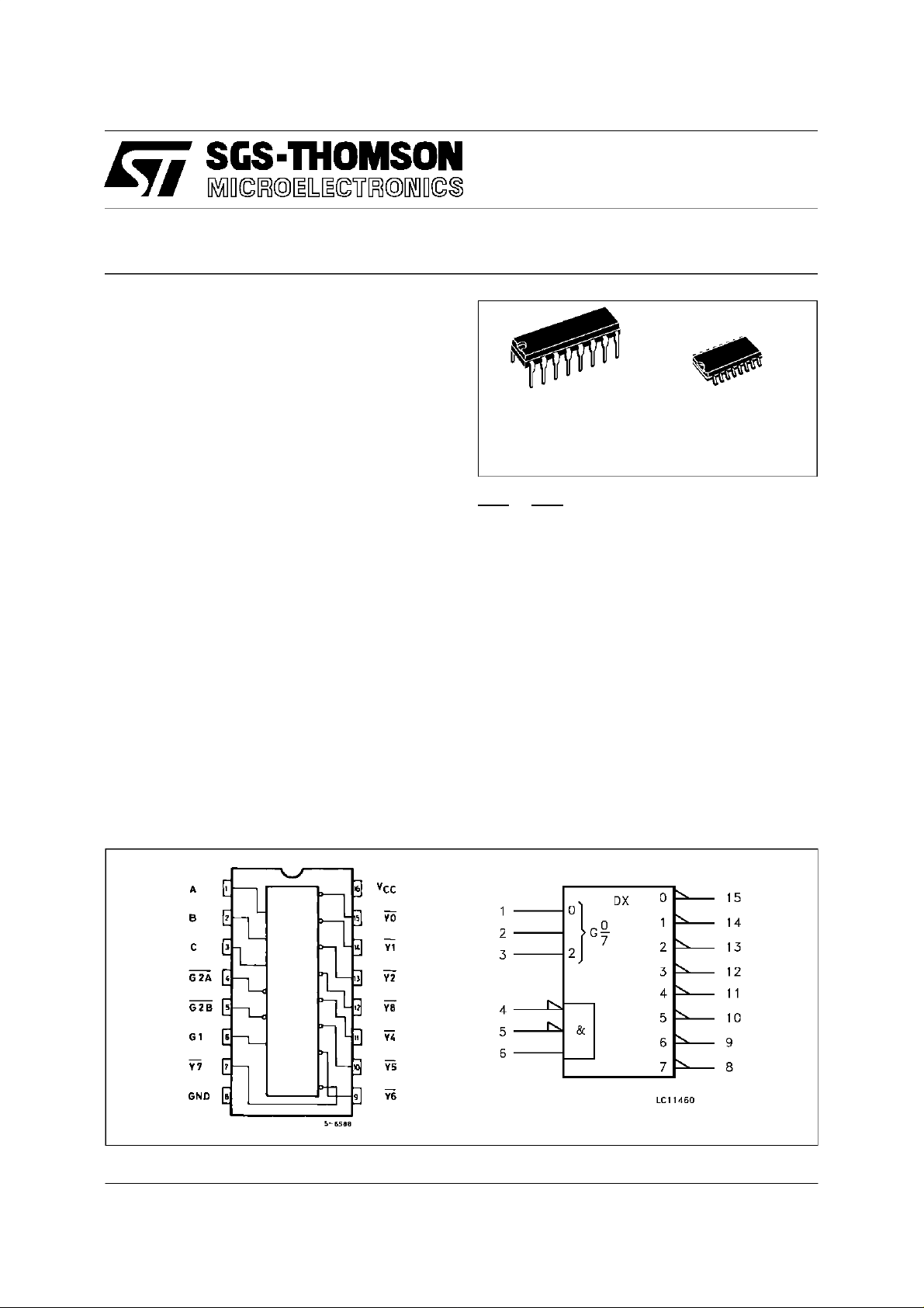
If the device is enabled, 3 binary select inputs (A,
B and C) determine which one of the outputs will
B
(Plastic Package)
(Micro Package)
M
ORDERCODES:
74AC138B
go low. If enable input G1 is held low or either
G2A or G2B is held high, the decoding function is
inhibitedand all the 8 outputsgoto high.
Tree enable inputs are provided to ease cascade
connection and application of address decoders
for memory systems.
It is ideal for low power applications mantaining
high speed operation similar to equivalent Bipolar
SchottkyTTL.
All inputs and outputs are equipped with
protectioncircuits against static discharge, giving
them 2KV ESD immunity and transient excess
voltage.
PINCONNECTION AND IEC LOGIC SYMBOLS
April 1997
1/9
74AC138
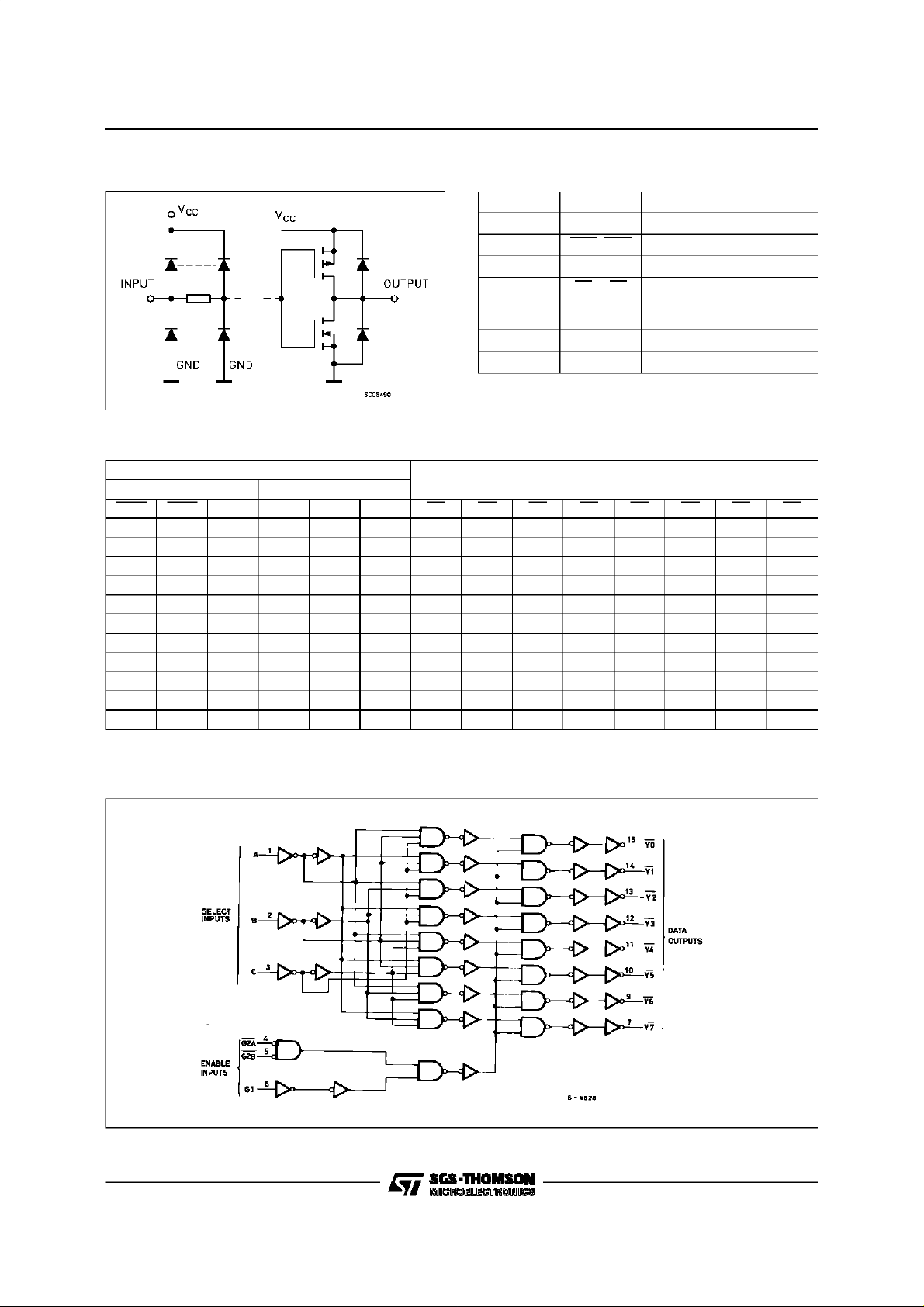
INPUTAND OUTPUTEQUIVALENTCIRCUIT
PIN DESCRIPTION
PI N No SYM B O L NAME A ND FUNCT I ON
1, 2, 3 A, B, C Address Inputs
4, 5 G2A, G2B Enable Inputs
6 G1 Enable Input
15, 14, 13,
12, 11, 10,
9, 7
8 GND Ground (0V)
16 V
Y0 to Y7 Outputs
CC
Positive Supply Voltage
TRUTH TABLE
INPUTS OUTPUTS
ENABLE SELEC T
G2B G2A G1 C B A Y0 Y1 Y2 Y3 Y4 Y5 Y6 Y7
XXLXXXHHHHHHHH
XHXXXXHHHHHHHH
HXXXXXHHHHHHHH
LLHLL LLHHHHHHH
LLHLLHHLHHHHHH
LLHLHLHHLHHHHH
LLHLHHHHHLHHHH
LLHHL LHHHHLHHH
LLHHLHHHHHHLHH
LLHHHLHHHHHHLH
LLHHHHHHHHHHHL
X:Don’t Care
LOGICDIAGRAM
This logic diagram has not be used to estimate propagation delays
2/9
74AC138
ABSOLUTE MAXIMUMRATINGS
Symb o l Parame t er Val u e Uni t
V
V
V
I
I
OK
I
orI
I
CC
T
T
Absolute Maximum Ratings are those values beyond which damage to the device may occur. Functional operation under these condition is not implied.
RECOMMENDED OPERATINGCONDITIONS
Symb o l Parame t er Value Un i t
V
V
V
T
dt/dv Input Rise and Fall Time V
1) VINfrom30% to70%ofV
Supply Voltage -0.5 to +7 V
CC
DC Input Voltage -0.5 to VCC+ 0.5 V
I
DC Output Voltage -0.5 to VCC+ 0.5 V
O
DC Input Diode Current ± 20 mA
IK
DC Output Diode Current ± 20 mA
DC Output Current ± 50 mA
O
DC VCCor Ground Current ± 400 mA
GND
Storage Temperature -65 to +150
stg
Lead Temperature (10 sec) 300
L
Supply Voltage 2 to 6 V
CC
Input Voltage 0 to V
I
Output Voltage 0 to V
O
Operating Temperature: -40 to +85
op
= 3.0, 4.5 or 5.5 V(note 1) 8 ns/V
CC
CC
CC
CC
o
C
o
C
V
V
o
C
3/9
 Loading...