

74AC02
QUAD 2-INPUT NOR GATE
■ HIGH SPEED: t
■ LOWPOWER DISSIPATION:
=4µA (MAX.) at TA=25oC
I
CC
■ HIGH NOISE IMMUNITY:
V
NIH=VNIL
■ 50Ω TRANSMISSIONLINE DRIVING
= 4.5 ns(TYP.) at VCC=5V
PD
=28%VCC(MIN.)
CAPABILITY
■ SYMMETRICAL OUTPUT IMPEDANCE:
|I
|=IOL=24 mA (MIN)
OH
■ BALANCEDPROPAGATIONDELAY S:
t
≅ t
PLH
PHL
■ OPERATINGVOLTAGERAN GE:
V
(OPR) = 2V to 6V
CC
■ PIN AND FUNCTION COMPATIBLE WITH
74SERIES02
■ IMPROVED LATCH-UP IMMUNITY
DESCRIPTION
The AC02 is an advanced high-speed CMOS
QUAD 2-INPUT NOR GATE fabricated with
sub-micron silicon gate and double-layer metal
B
(Plastic Package)
(Micro Package)
M
ORDERCODES:
74AC02B 74AC02M
wiring C
2
MOS technology. It is ideal for low
power applications mantaining high speed
operation similar to equivalent Bipolar Schottky
TTL.
The internal circuit is composed of 3 stages
including buffer output, which enables high noise
immunityand stableoutput.
All inputs and outputs are equipped with
protectioncircuits against static discharge, giving
them 2KV ESD immunity and transient excess
voltage.
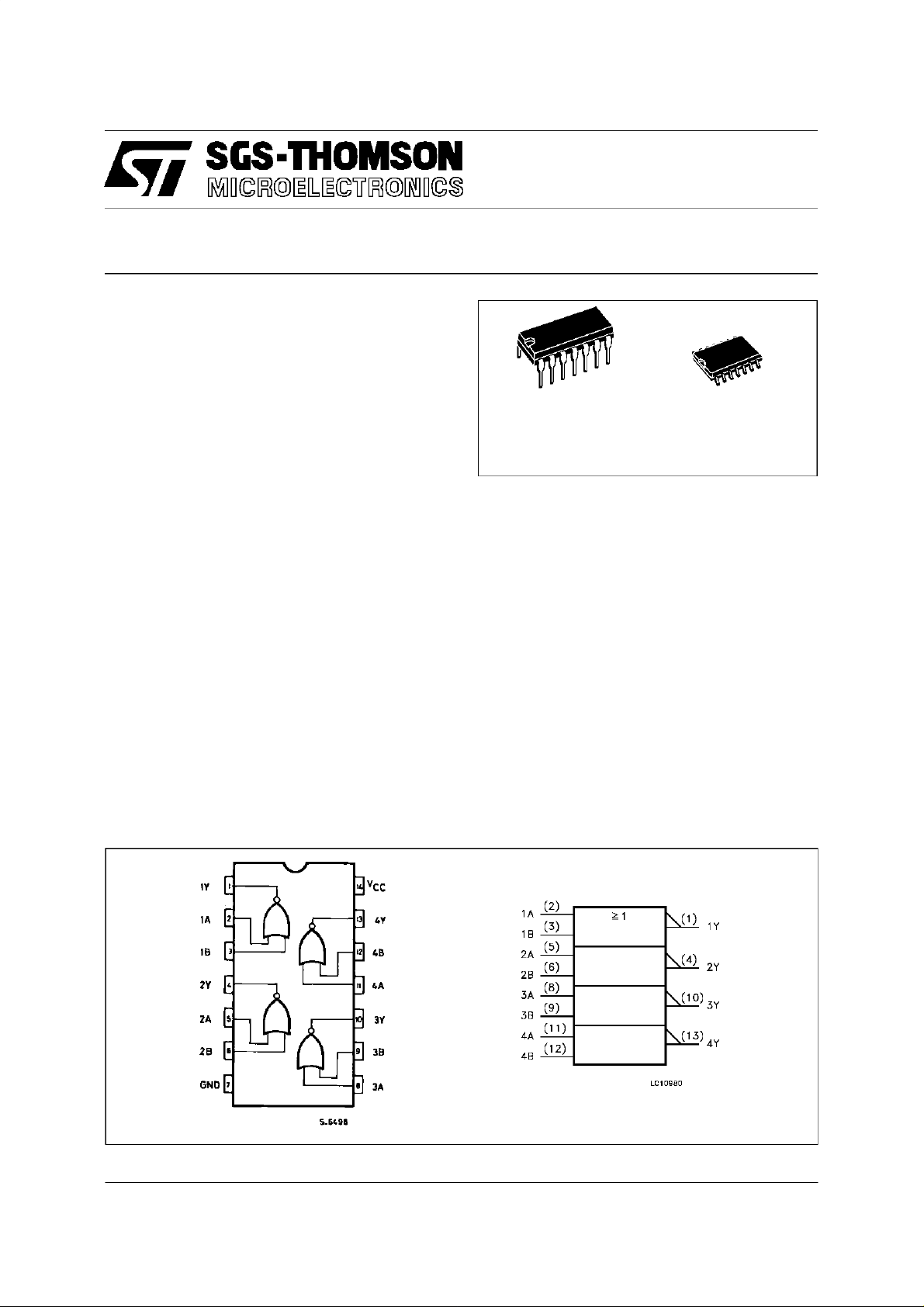
PINCONNECTION AND IEC LOGICSYMBOLS
April 1997
1/7
74AC02
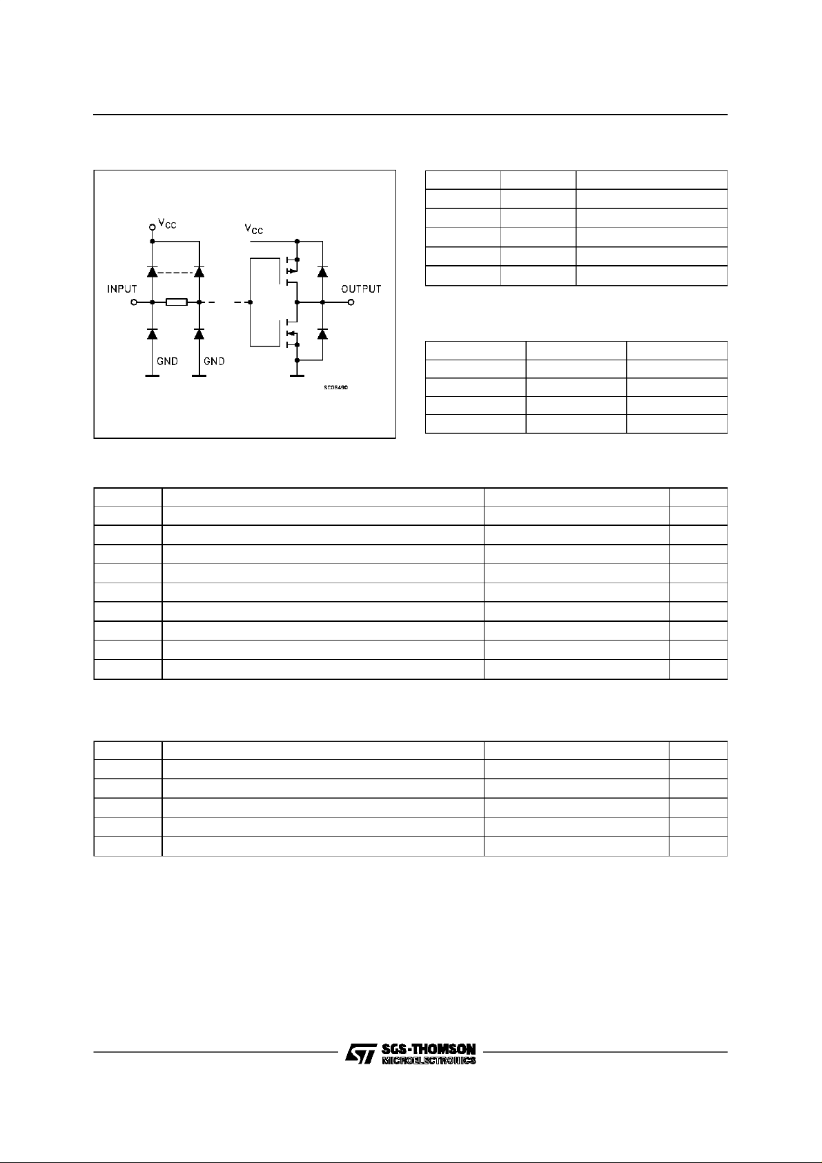
INPUTAND OUTPUTEQUIVALENTCIRCUIT
PIN DESCRIPTION
PI N No SYM B O L NAME AND FUNCT I ON
2, 5, 8, 11 1A to 4A Data Inputs
3, 6, 9, 12 1B to 4B Data Inputs
1, 4, 10, 12 1Y to 4Y Data Outputs
7 GND Ground (0V)
14 V
CC
Positive Supply Voltage
TRUTHTABLE
ABY
LLH
LHL
HLL
HHL
ABSOLUTE MAXIMUM RATINGS
Symb o l Parame t er Val u e Uni t
V
V
V
I
I
OK
I
orI
I
CC
T
T
Absolute Maximum Ratings are those values beyond which damage to the device may occur. Functional operation under these condition is not implied.
Supply Voltage -0.5 to +7 V
CC
DC Input Voltage -0.5 to VCC+ 0.5 V
I
DC Output Voltage -0.5 to VCC+ 0.5 V
O
DC Input Diode Current ± 20 mA
IK
DC Output Diode Current ± 20 mA
DC Output Current ± 50 mA
O
DC VCCor Ground Current ± 200 mA
GND
Storage Temperature -65 to +150
stg
Lead Temperature (10 sec) 300
L
o
C
o
C
RECOMMENDED OPERATINGCONDITIONS
Symb o l Parame t er Value Un i t
V
V
V
T
dt/dv Input Rise and Fall Time V
1) VINfrom30%to70%of V
2/7
Supply Voltage 2 to 6 V
CC
Input Voltage 0 to V
I
Output Voltage 0 to V
O
Operating Temperature: -40 to +85
op
= 3.0, 4.5 or 5.5 V(note 1) 8 ns/V
CC
CC
CC
CC
V
V
o
C
DC SPECIFICATIONS
74AC02
Symbol Parameter Test Condition s Value Unit
V
CC
(V)
High Level Input Voltage 3.0 VO= 0.1 V or
V
IH
4.5 3.15 2.25 3.15
V
CC
- 0.1 V
T
=25oC-40to85
A
Min. Typ. Max. Min . Max.
2.1 1.5 2.1
o
C
5.5 3.85 2.75 3.85
Low Level Input Voltage 3.0 VO= 0.1 V or
V
IL
4.5 2.25 1.35 1.35
V
CC
- 0.1 V
1.5 0.9 0.9
5.5 2.75 1.65 1.65
High Level Output
V
OH
Voltage
Low Level Output
V
OL
Voltage
Input Leakage Current
I
I
Quiescent Supply
I
CC
3.0
4.5 I
5.5 I
V
V
3.0 I
4.5 I
5.5 I
3.0
4.5 I
5.5 I
V
V
3.0 I
4.5 I
5.5 I
5.5
IO=-50 µA 2.9 2.99 2.9
(*)
I
IH
V
IL
=-50 µA 4.4 4.49 4.4
O
=
=-50 µA 5.4 5.49 5.4
or
O
=-12 mA 2.56 2.46
O
=-24 mA 3.86 3.76
O
=-24 mA 4.86 4.76
O
IO=50 µA 0.002 0.1 0.1
(*)
I
IH
V
IL
=50 µA 0.001 0.1 0.1
O
=
=50 µA 0.001 0.1 0.1
or
O
=12 mA 0.36 0.44
O
=24 mA 0.36 0.44
O
=24 mA 0.36 0.44
O
VI=VCCor GND ±0.1 ±1 µA
5.5 VI=VCCor GND 4 40 µA
Current
Dynamic Output Current
I
OLD
OHD
(note 1, 2)
I
1) Maximum test duration 2ms, one output loaded at time
2) Incident wave switching is guaranteed on transmission lines with impedances aslow as 50 Ω.
(*)All outputs loaded.
5.5 V
= 1.65 V max 75 mA
OLD
V
= 3.85 V min -75 mA
OHD
V
V
V
V
AC ELECTRICAL CHARACTERISTICS (CL= 50 pF, RL=500 Ω, Inputtr=tf=3ns)
Symbol Parameter Test Conditi on Value Unit
t
Propagation Delay Time 3.3
PLH
t
PHL
(*) Voltagerangeis 3.3V± 0.3V
(**) Voltagerangeis5V± 0.5V
V
5.0
CC
(V)
(*)
(**)
T
=25oC-40to85
A
Min. Typ. Max. Min . Max.
1.5 5.5 7.5 1 8
1.5 4.5 6.5 1 7
o
C
ns
CAPACITIVE CHARACTERISTICS
Symbol Parameter Test Condition s Value Unit
=25oC-40to85
T
A
Min. Typ. Max. Min . Max.
4
Input Capacitance
C
IN
Power Dissipation
C
PD
V
CC
(V)
5.0
5.0 46 pF
Capacitance (note 1)
1) CPDis defined as the value of the IC’s internal equivalent capacitance which is calculated from the operating current consumption without load. (Refer to
Test Circuit). Average operating current can be obtained by the following equation. I
(opr) = CPD• VCC•fIN+ICC/n (percircuit)
CC
o
C
pF
3/7
 Loading...