

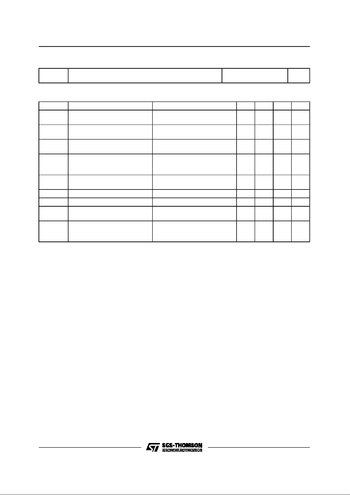
DESCRIPTIO N
The 2N5415S is a silicon planar epitaxial PNP transistorinJedec TO-39 metalcase, intended for high
vol-tageswitching and linear amplifier applications.
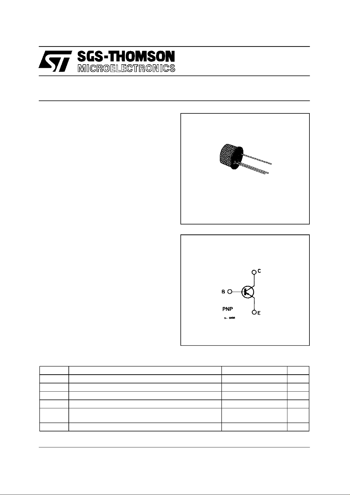
2N5415S
HIGH-VOLTAGE AMPLIFIER
TO-39
INTE RNA L SCHEMA TI C DIAGR AM
ABSOLUTE MA XIMUM RATI NG S
Symbol Parameter Valu e Unit
V
CBO
V
CEO
V
EBO
I
CM
P
T
stg,Tj
tot
Collector-base Voltage (IE= 0) – 200 V
Collector-emitter Voltage (IB= 0) – 200 V
Emitter-base Voltage (IC=0) –4 V
Collector Peak Current – 1 A
Total Power Dissipation at T
at T
Storage and Junction Temperature – 55 to 200 °C
amb
case
≤ 25 °C
≤ 25 °C
1
10
W
W
October 1988
1/4
2N5415S
THERMAL DATA
R
th j-case
R
th j-amb
ELECTRICAL CHARACTERISTICS (T
Thermal Resistance Junction-case
Thermal Resistance Junction-ambient
amb
Max
Max
=25°C unless otherwise specified)
17.5
175
Symbol Parameter Test Conditions Min. Typ. Max. Unit
I
CBO
Collector Cutoff Current
VCB= – 175 V – 50 µA
(IE=0)
V(
V
I
CEO
I
EBO
BR)CEO
CE(sa t)
Collector Cutoff Current
(I
=0)
B
Emitter Cutoff Current
(I
=0)
C
* Collector-emitter
Breakdown Voltage
(I
=0)
B
* Collector-emitter
= – 150 V – 50 µA
V
CE
=–4V –20 µA
V
EB
IC=–2mA –200 V
Saturation Voltage IC= – 50 mA IB= – 5 mA – 2.5 V
V
* Base-Emitter Voltage IC= – 50 mA VCE= – 10 V – 1.5 V
BE
h
* DC Current Gain IC=–50A VCE= – 10 V 30 150
FE
f
T
C
CBO
* Pulsed : pulse duration = 300 µs, duty cycle = 1 %.
Transition Frequency IC=–10mA
f=5MHz
Collector-base
Capacitance IE=0
f=1MHz
VCE=–10V
15 MHz
VCB=–10V
15 pF
°C/W
°C/W
2/4
 Loading...