

The documentation and process
INCH-POUND
conversion measures necessary to
comply with this revision shall be
completed by 31 November 2000.
MIL-PRF-19500/376E
31 August 2000
SUPERSEDING
MIL-PRF-19500/376D
21 August 1998
PERFORMANCE SPECIFICATION
SEMICONDUCTOR DEVICE, TRANSISTOR, NPN, SILICON, LOW-POWER
TYPES 2N2484, 2N2484UA, 2N2484UB, JAN, JANTX, JANTXV, JANS, JANHC, AND JANKC
This specification is approved for use by all Departments
and Agencies of the Department of Defense.
1. SCOPE
1.1 Scope. This specification covers the performance requirements for NPN, silicon, low-power transistors.
Four levels of product assurance is provided for each device type as specified in MIL-PRF-19500. Two levels of
product assurance are provided for die.
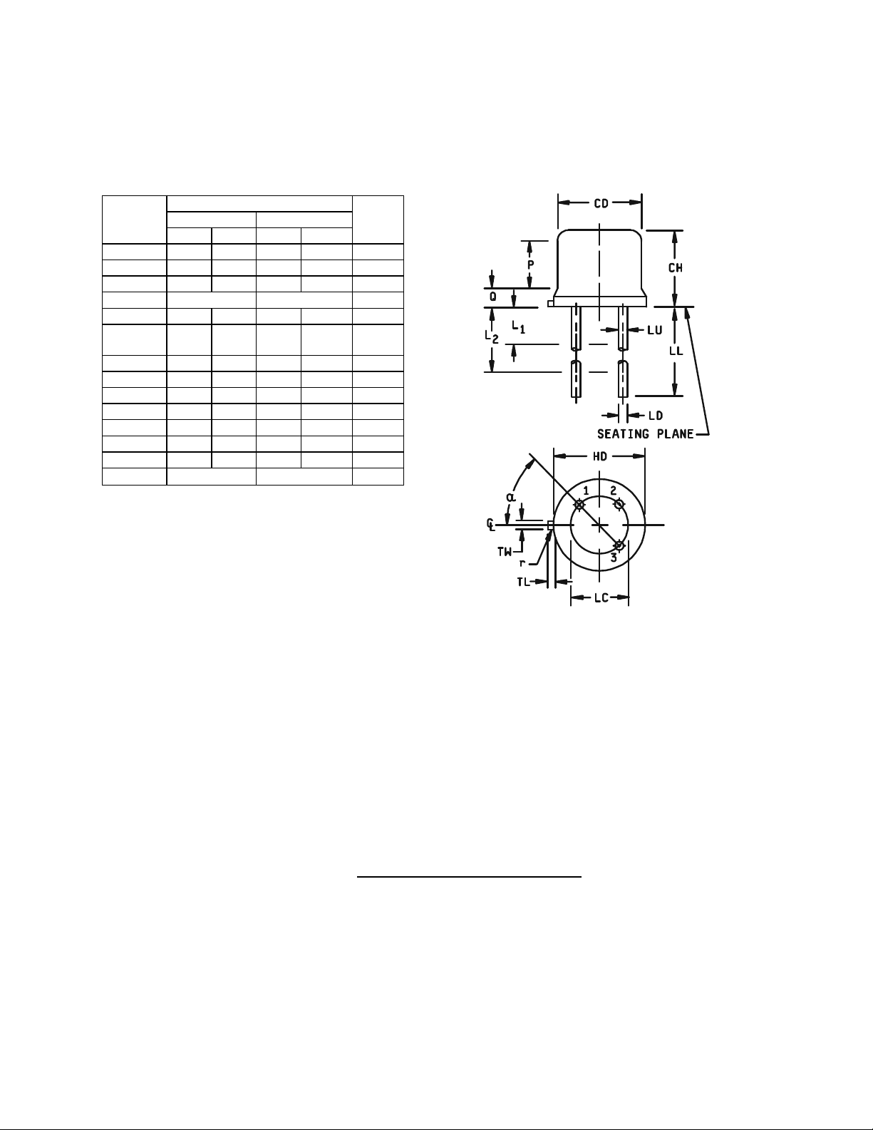
1.2 Physical dimensions. See figure 1 (similar to T0-18), figures 2 and 3 (surface mount case outlines UA and
UB), and figures 4 and 5 (die).
1.3 Maximum ratings.
Types
2N2484 500 (1) 60 6 60 50 -65 to +200 325 146
2N2484UA 650 (2) 60 6 60 50 -65 to +200 210 160
2N2484UB 500 (1) 60 6 60 50 -65 to +200 325 146
P
T
TA = +25°C
mW V dc V dc V dc mA dc
V
CBO
V
EBO
V
CEO
I
C
TJ and T
STG
°C °C/W °C/W
R
θJA
R
θJC
(1) Derate linearly at 3.08 mW/°C above TA = +37.5°C
(2) Derate linearly at 4.76 mW/°C above TA = +63.5°C.
1.4 Primary electrical characteristics.
Limits
Min
Max
h
fe
VCE = 5 V dc
IC = 1 mA dc
f = 1 kHz
250
900
C
obo
IE = 0
VCB = 5 V dc
100 kHz ≤ f ≤ 1 MHz
pF
5.0
|hfe|2 V
IC = 500 µA dc
VCE = 5 V dc
f = 30 MHz
2.0
7.0
(1)
CE(sat)
IC = 1.0 mA dc
IB = 0.1 mA dc
V dc
0.3
(1) Pulsed (see 4.5.1).
Beneficial comments (recommendations, additions, deletions) and any pertinent data which may be of use in
improving this document should be addressed to: Defense Supply Center, Columbus, ATTN: DSCC/VAC,
Post Office Box 3990, Columbus, OH 43216-5000, by using the Standardization Document Improvement Proposal
(DD Form 1426) appearing at the end of this document or by letter.
AMSC N/A FSC 5961
DISTRIBUTION STATEMENT A. Approved for public release; distribution is unlimited.
MIL-PRF-19500/376E
Dimensions
Symbol Inches Millimeters Note
Min Max Min Max
CD .178 .195 4.52 4.95
CH .170 .210 4.32 5.33
HD .209 .230 5.31 5.84
LC .100 TP 2.54 TP 6
LD .016 .021 0.41 0.53 7,8
LL .500 .750 12.7019.05 7,8
LU .016 .019 0.41 0.48 7,8
L1 --- .050 --- 1.27 7,8
L2 .250 --- 6.35 --- 7,8
Q --- .040 --- 0.86 5
TL .028 .048 0.71 1.22 3,4
TW .036 .046 0.91 1.17 3
r --- .010 --- 0.25 10
α 45° TP 45° TP
6
NOTES:
1. Dimension are in inches.
2. Metric equivalents are given for general information only.
3. Beyond r (radius) maximum, TW shall be held for a minimum length of .011 (0.28 mm).
4. Dimension TL measured from maximum HD.
5. Body contour optional within zone defined by HD, CD, and Q.
6. Leads at gauge plane .054 +.001 -.000 inch (1.37 +0.03 -0.00 mm) below seating plane shall
be within .007 inch (0.18 mm) radius of true position (TP) at maximum material condition
(MMC) relative to tab at MMC.
7. Dimension LU applies between L1 and L2. Dimension LD applies between L2 and LL
minimum. Diameter is uncontrolled in L1 and beyond LL minimum.
8. All three leads.
9. The collector shall be internally connected to the case.
10. Dimension r (radius) applies to both inside corners of tab.
11. In accordance with ANSI Y14.5M, diameters are equivalent to φx symbology.
12. Lead 1 = emitter, lead 2 = base, lead 3 = collector.
FIGURE 1. Physical dimensions (similar to TO-18).
2
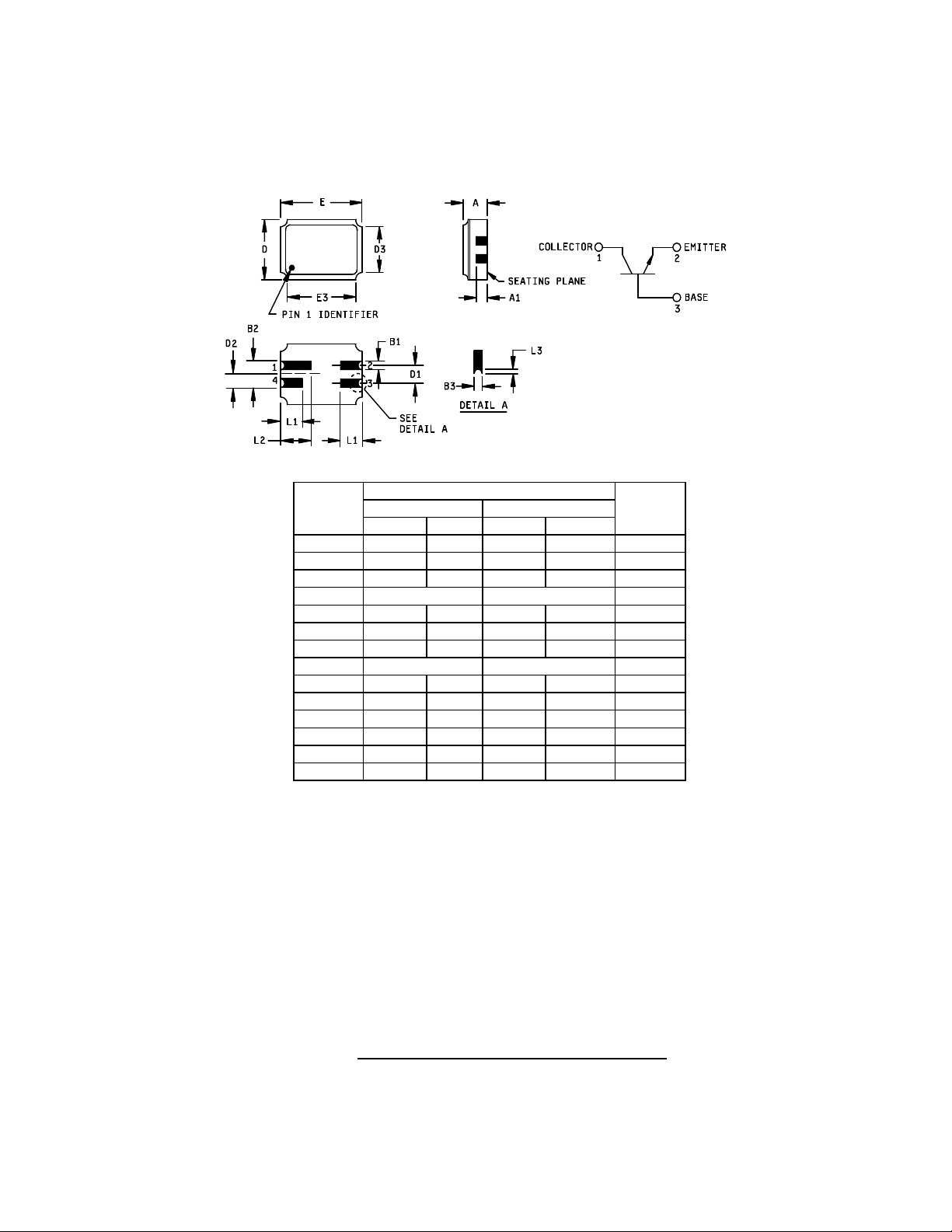
MIL-PRF-19500/376E
Dimensions
Symbol Inches Millimeters Note
Min Max Min Max
A .061 .075 1.55 1.90 3
A1 .029 .041 0.74 1.04
B1 .022 .028 0.56 0.71
B2 .075 REF 1.91 REF
B3 .006 .022 0.15 0.56 5
D .145 .155 3.68 3.93
D1 .045 .055 1.14 1.39
D2 .0375 BSC .952 BSC
D3 --- .155 --- 3.93
E .215 .225 5.46 5.71
E3 --- .225 --- 5.71
L1 .032 .048 0.81 1.22
L2 .072 .088 1.83 2.23
L3 .003 .007 0.08 0.18 5
NOTES:
1. Dimensions are in inches.
2. Metric equivalents are given for general information only.
3. Dimension "A" controls the overall package thickness. When a window lid is used, dimension "A" must
increase by a minimum of .010 inch (0.254 mm) and a maximum of .040 inch (1.020 mm).
4. The corner shape (square, notch, radius, etc.) may vary at the manufacturer's option, from that shown on
the drawing.
5. Dimensions "B3" minimum and "L3" minimum and the appropriately castellation length define an
unobstructed three-dimensional space traversing all of the ceramic layers in which a castellation was
designed. (Castellations are required on bottom two layers, optional on top ceramic layer.) Dimension
"B3" maximum and "L3" maximum define the maximum width and depth of the castellation at any point on
its surface. Measurement of these dimensions may be made prior to solder dipping.
6. Lead 4 = no connection.
FIGURE 2. Physical dimensions, surface mount (2N2484UA).
3
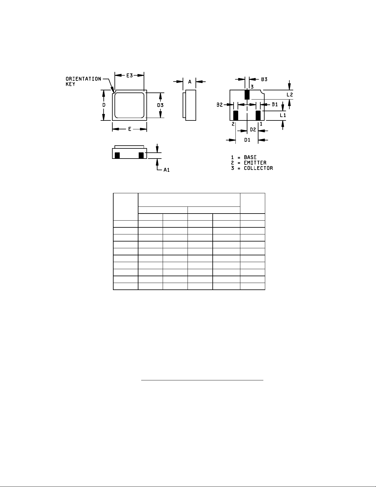
MIL-PRF-19500/376E
Dimensions
Inches Millimeters
Min. Max. Min. Max.
A .046 .056 0.97 1.42
A1 .017 .035 0.43 0.89
B1 .016 .024 0.41 0.61 3
D .085 .108 2.41 2.74
D1 .071 .079 1.81 2.01
D2 .035 .039 0.89 0.99
D3
E .115 .128 2.82 3.25
E3
L1 .022 .038 0.56 0.96 4
NOTES:
1. Dimensions are in inches.
2. Metric equivalents are given for general information only.
3. Dimensions B2 and B3 are identical to B1
4. Dimension L2 is identical to L1.
FIGURE 3. Physical dimensions, surface mount (2N2484UB).
NotesLtr
4
MIL-PRF-19500/376E
A- version
NOTES:
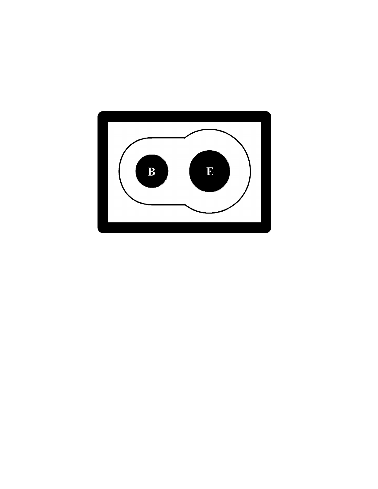
1. Die size...............................................0.015 x 0.019 inches ± 0.001 inch
2. Die thickness.......................................0.010 ± 0.0015 inches
3. Top metal............................................Aluminum 15,000Å minimum, 18,000Å nominal
4. Back metal ..........................................A. Gold 2,500Å minimum, 3,000Å nominal
B. Eutectic Mount – No Gold
5. Backside.............................................Collector
6. Bonding pad........................................ B = 0.003 inches, E = 0.004 inches diameter
7. Passivation.........................................Si3N4 (Silicon Nitride) 2kÅ min, 2.2kÅ nom.
FIGURE 4. Physical dimensions, JANHC and JANKC die, A - version.
5
MIL-PRF-19500/376E
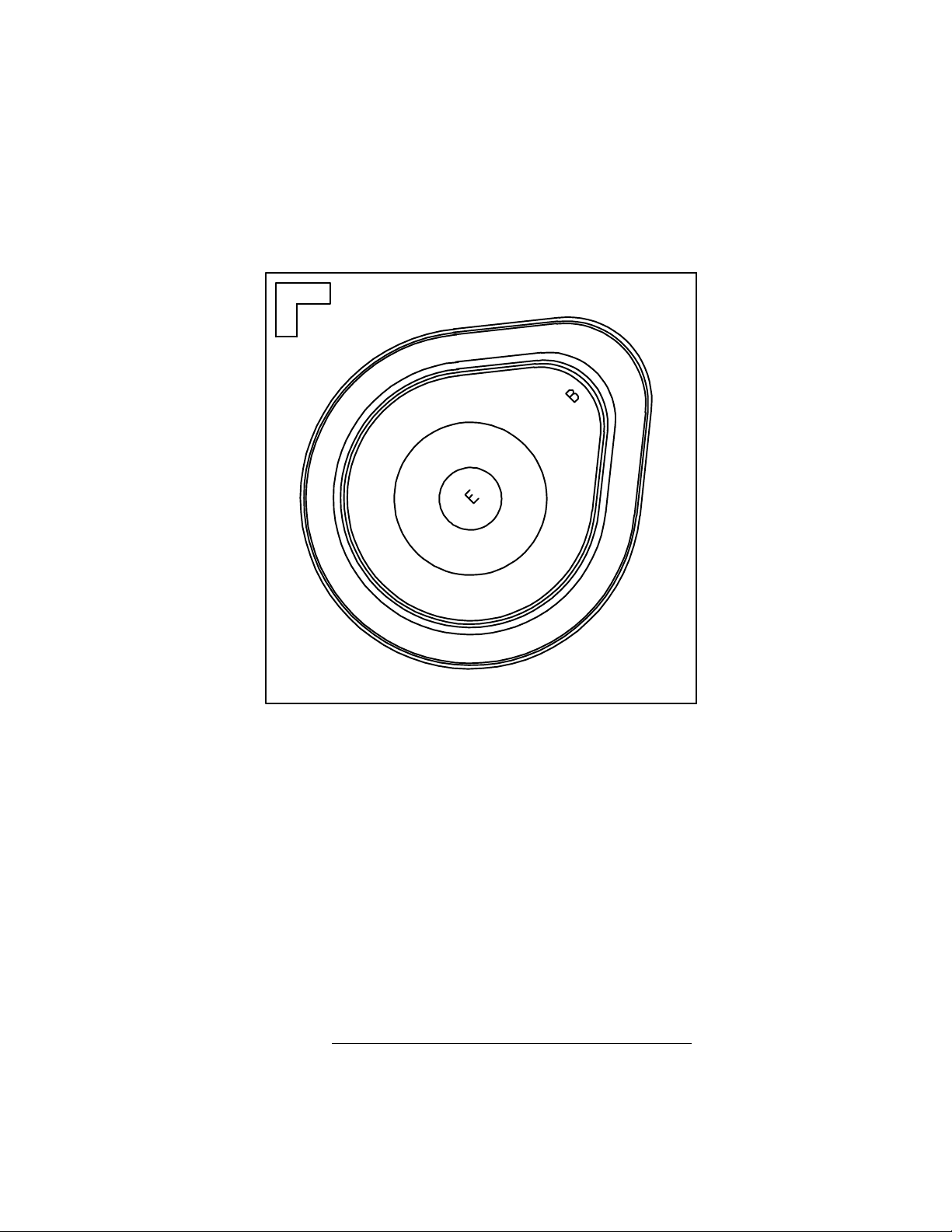
B - version
Die size:.....................................................0.018 x 0.018 inches
Die thickness: ............................................ 0.008 ± 0.0016 inches
Base pad: .................................................. 0.0025 inches diameter
Emitter pad:............................................... 0.003 inches diameter
Back metal:................................................ Gold, 6500 ± 1950 Å
Top metal: ................................................. Aluminum, 19500 ± 2500 Å
Back side:..................................................Collector
Glassivation:..............................................SiO2, 7500 ± 1500 Å
FIGURE 5. Physical dimensions, JANHC and JANKC die, B - version.
6
 Loading...