

SGS Thomson Microelectronics 2N2222, 2N2221, 2N2219, 2N2218 Datasheet
DESCRIPTION
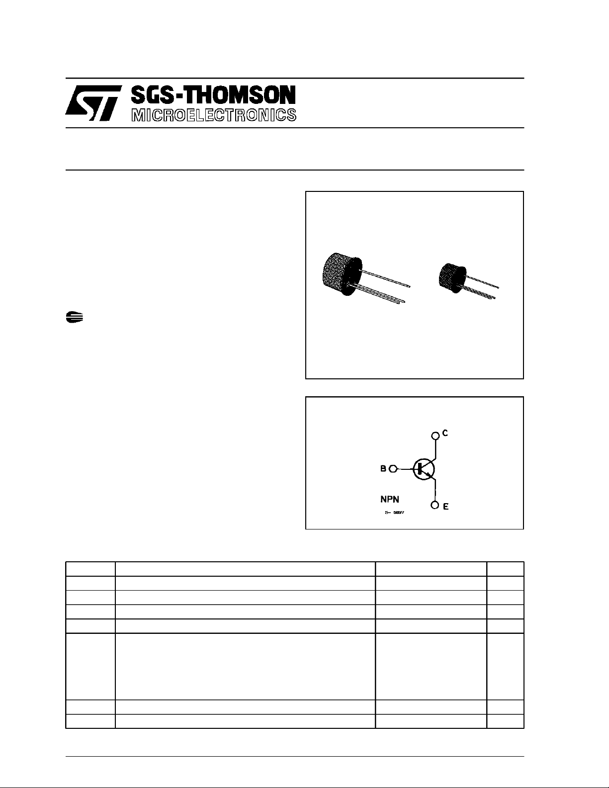
The 2N2218, 2N2219,2N2221 and 2N2222aresilicon planar epitaxial NPN transistors in Jedec
TO-39 (for 2N2218 and 2N2219) and in Jedec
TO-18(for2N2221 and2N2222) metalcases. They
are designed for high-speed switchingapplications
at collectorcurrents upto 500 mA, and featureuseful current gain over a wide range of collector current, low leakage currents and low saturation voltages.
2N2218-2N2219
2N2221-2N2222
HIGH-SPEED SWITCHES
2N2218/2N2219 approved to CECC 50002100, 2N2221/2N2222 approved to CECC
TO-39
TO-18
50002-101 available on request.
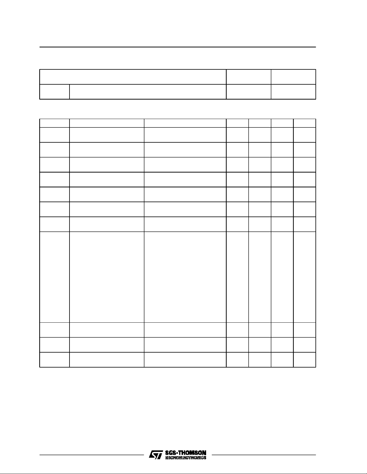
INTERNAL SCHEMATIC DIAGRAM
ABSOLUTE MAXIMUM RATIN G S
Symbol Parameter Value Unit
V
V
V
P
T
CBO
CEO
EBO
I
C
tot
stg
T
Collector-base Voltage (IE=0) 60 V
Collector-emitter Voltage (IB=0) 30 V
Emitter-base Voltage (IC=0) 5 V
Collector Current 0.8 A
Total Power Dissipation at T
for 2N2218 and 2N22 19
for 2N2221 and 2N22 22
at T
for 2N2218 and 2N22 19
for 2N2221 and 2N22 22
Storage Temperature – 65 to 200 °C
Junction Temperature 175 °C
j
amb
case
≤ 25 °C
0.8
0.5
≤ 25 °C
3
1.8
W
W
W
W
January 1989
1/5
2N2218-2N2219-2N2221-2N2222
THERMAL DATA
R
th j-case
R
th j-amb
Thermal Resistance Junction-case
Thermal Resistance Junction-ambient
ELECTRICAL CHARACTERISTICS (T
Max
Max
=25°C unless otherwise specified)
amb
2N22 18
2N22 19
50 °C/W
187.5 °C/W
2N222 1
2N222 2
83.3 °C/W
300 °C/W
Symbol Parameter Test Conditions Min. Typ. Max. Unit
I
CBO
I
EBO
V
(BR) CBO
V
(BR)CEO
V
(BR) EBO
V
CE (sat )
V
BE (sat )
h
FE
f
T
C
CBO
R
e(hie)
*
Pulsed : pulse duration = 300 µs, duty cycle = 1 %.
Collector Cutoff Current
(I
=0)
E
Emitter Cutoff Current
(I
=0)
C
Colllector-base Breakdown
Voltage (IE=0)
* Collector-emitter Breakdown
Voltage (IB=0)
Emittter-base Breakdown
Voltage (IC=0)
* Collector-emitter Saturation
Voltage
* Base-emitter Saturation
Voltage
=50V
V
CB
V
=50V T
CB
=3V 10 nA
V
EB
=10µA60V
I
C
I
=10mA 30 V
C
I
=10µA5V
E
IC=150mA
IC=500mA
IC=150mA
I
=500mA
C
* DC Current Gain for 2N2218
I
= 0.1 mA
C
IC=1mA
I
=10mA
C
IC=150mA
IC=500mA
I
=150mA
C
for 2N2219
I
= 0.1 mA
C
IC=1mA
IC=10mA
I
=150mA
C
IC=500mA
I
=150mA
C
Transition Frequency IC=20mA
f = 100 MHz
Collector-base Capacitance IE=0
f = 100 kHz
Real Part of Input
Impedance
IC=20mA
f = 300 MHz
=150°C
amb
IB=15mA
IB=50mA
=15mA
I
B
I
=50mA
B
and 2N2221
V
=10V
CE
VCE=10V
V
=10V
CE
VCE=10V
VCE=10V
V
=1V
CE
and 2N2222
V
=10V
CE
VCE=10V
VCE=10V
V
=10V
CE
VCE=10V
V
=1V
CE
V
= 20 V 250 MHz
CE
V
=10V 8 pF
CB
=20V 60 Ω
V
CE
20
25
35
40
20
20
35
50
75
100
30
50
10
10
0.4
1.6
1.3
2.6
120
300
nA
µA
V
V
V
V
2/5
 Loading...