

查询VNW50N04A供应商
FULLY AUTOPROTECTED POWER MOSFET
VNW50N04A
”OMNIFET”:
TYPE V
VNW50 N04 A 42 V 0.012 Ω 50 A
■ LINEARCURRENTLIMITATION
■ THERMALSHUT DOWN
■ SHORTCIRCUIT PROTECTION
■ INTEGRATEDCLAMP
■ LOW CURRENT DRAWN FROM INPUTPIN
■ DIAGNOSTICFEEDBACK THROUGHINPUT
clamp
R
DS(on)
I
lim
PIN
■ ESDPROTECTION
■ DIRECTACCESS TO THE GATE OF THE
POWERMOSFET (ANALOG DRIVING)
■ COMPATIBLEWITH STANDARD POWER
MOSFET
■ STANDARDTO-247 PACKAGE
DESCRIPTION
The VNW50N04A is a monolithic device made
using SGS-THOMSON Vertical Intelligent Power
M0 Technology, intended for replacement of
standard power MOSFETS in DC to 50 KHz
applications. Built-in thermal shut-down, linear
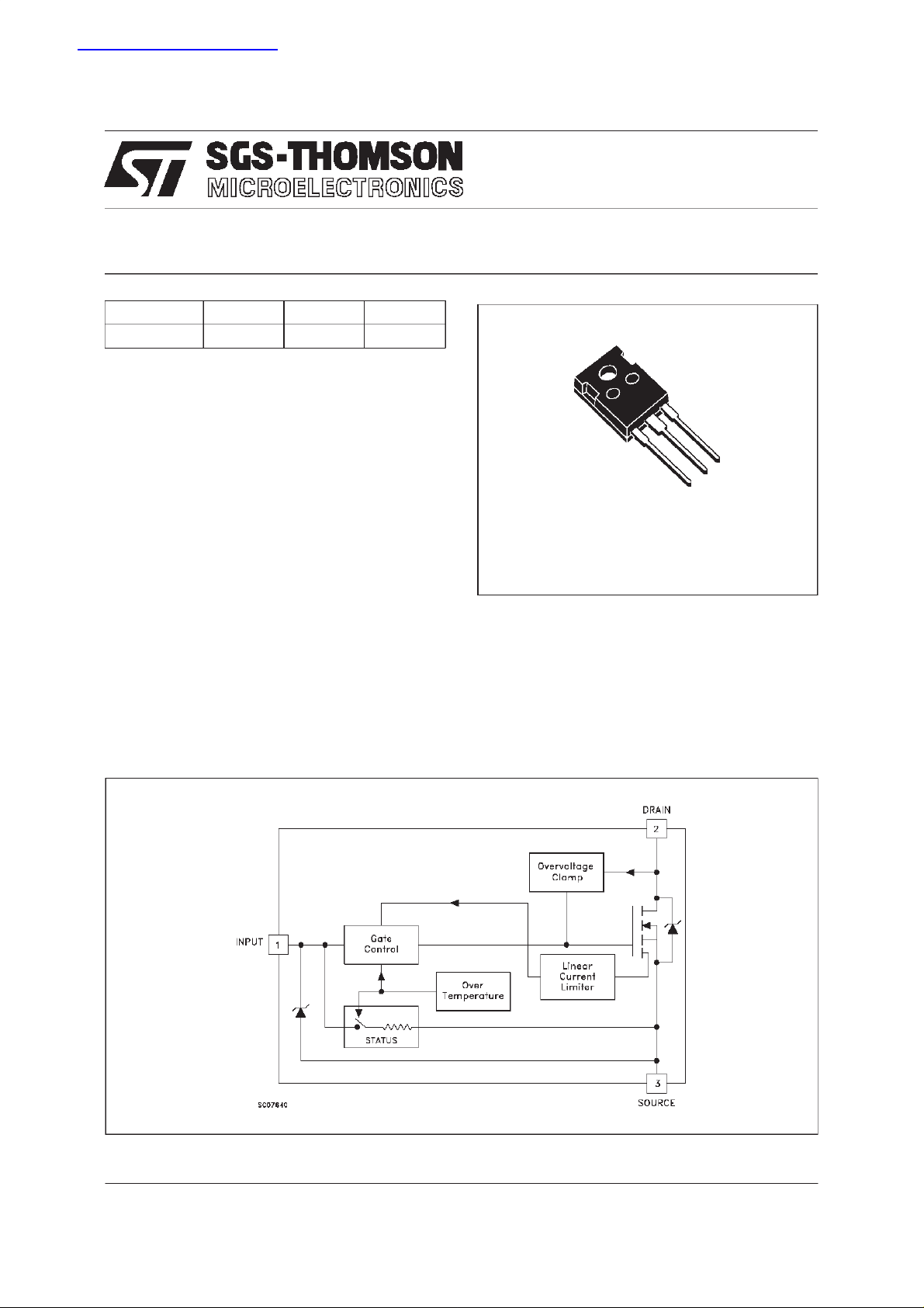
BLOCK DIAGRAM
3
2
1
TO-247
current limitation and overvoltage clamp protect
the chip in harsh enviroments.
Faultfeedback can be detectedby monitoringthe
voltageat theinput pin.
February 1998
1/11

VNW50N04A
ABSOLUTEMAXIMUM RATING
Symbol Parameter Value Unit
V
V
V
P
T
THERMAL DATA
R
thj-case
R
thj-amb
Drain-source Voltage (Vin= 0) Int er nall y Clamped V
DS
Input Voltage 18 V
in
I
Drain Current Internally Limited A
D
I
Reverse DC Out put Current -100 A
R
Elect r o st at ic Discharge (C= 100 pF , R=1.5 KΩ) 2000 V
esd
Tot al Dissipation at Tc=25oC 208 W
tot
T
Oper at i ng Junct ion Temperat ure Internally Limited
j
T
Case Operating Temperature Internally Limited
c
St orage Temperature -55 t o 150
stg
Ther mal Resis t ance Junct io n- case Max
Ther mal Resis t ance Junct io n- ambien t Max
0.6
30
o
o
o
C
o
C
o
C
C/W
C/W
ELECTRICAL CHARACTERISTICS (T
=25oC unlessotherwise specified)
case
OFF
Symbol Parameter Test Conditions Min. Typ. Max. Unit
V
CLAMP
Drain-source Clamp
ID=18A Vin= 0 36 42 48 V
Volt age
V
CLTH
Drain-source Clamp
ID=2mA Vin=0 35 V
Thr eshold Volta ge
V
INCL
Input-Source Reverse
Iin=-1mA -1 -0.3 V
Clamp Voltage
I
DSS
I
ISS
Zer o I npu t V olt age
Drain Current (V
in
Supply Current from
=0)
=13V Vin=0
V
DS
V
=25V Vin=0
DS
50
200
VDS=0V Vin= 10 V 250 500 µA
Input Pin
ON (∗)
Symbol Parameter Test Conditions Min. Typ. Max. Unit
V
IN(th)
Input Thres hold
VDS=VinID+Iin=1mA 0.8 3 V
Volt age
R
DS(on)
St at ic Drain-source On
Resistance
Vin=10V ID=25A
=5V ID=25A
V
in
0.012
0.015ΩΩ
DYNAMIC
µA
µA
Symbol Parameter Test Conditions Min. Typ. Max. Unit
g
(∗)Forward
fs
VDS=13V ID=25A 35 50 S
Tr ansc on ductance
C
Out put Capacit anc e VDS=13V f=1MHz Vin= 0 2000 3000 pF
oss
2/11

VNW50N04A
ELECTRICAL CHARACTERISTICS (continued)
SWITCHING(∗∗)
Symbol Parameter Test Conditions Min. Typ. Max. Unit
t
d(on)
t
d(off)
t
d(on)
t
d(off)
(di/dt)
Q
Turn-on Delay Time
t
Rise Time
r
Turn-off Delay T ime
t
Fall T ime
f
Turn-on Delay Time
Rise Time
t
r
Turn-off Delay T ime
t
Fall T ime
f
Tur n-on Current Slope VDD=15V ID=25A
on
Total Input Charge VDD=15V ID=25A Vin= 10 V 190 nC
i
VDD=15V Id=25A
=10V R
V
gen
gen
=10Ω
(see figure 3)
VDD=15V Id=25A
V
=10V R
gen
= 1000 Ω
gen
(see figure 3)
=10V R
V
in
gen
=10Ω
SOURCE DRAIN DIODE
Symbol Parameter Test Conditions Min. Typ. Max. Unit
V
(∗)ForwardOnVoltage ISD=25A Vin=0 1.6 V
SD
Q
I
RRM
t
rr
Reverse Re covery
(∗∗)
Time
Reverse Re covery
(∗∗)
rr
Charge
(∗∗)
Reverse Re covery
Current
I
= 25 A di/dt = 100 A/µs
SD
V
=30V Tj=25oC
DD
(see test circuit, figure 5)
100
400
800
500
1.8
18
10
200
700
1500
900
3
3
5
25
15
55 A/µs
800
5
15
ns
ns
ns
ns
µs
µs
µs
µs
ns
µC
A
PROTECTION
Symbol Parameter Test Conditions Min. Typ. Max. Unit
t
dlim
T
jsh
I
lim
Drain Current Limit Vin=10V VDS=13V
=5V VDS=13V
V
in
(∗∗) St ep Response
Current Lim it
Vin=10V
=5V
V
in
(∗∗) O v er t emperature
Shut dow n
(∗∗) Overtemper at u r e Reset 135
T
jrs
I
(∗∗) Fault Sink Current Vin=10V VDS=13V
gf
E
(∗∗) S i ngle Pulse
as
Avalanche E nergy
(∗) Pulsed: Pulse duration = 300 µs, duty cycle1.5 %
(∗∗) Parametersguaranteed by design/characterization
=5V VDS=13V
V
in
starting Tj=25oCVDD=20V
=10V R
V
in
=1KΩ L=10mH
gen
35
35
50
50
65
65
50
13080200
150
50
20
4J
A
A
µs
µs
o
C
o
C
mA
mA
3/11

VNW50N04A
PROTECTION FEATURES
During normal operation, the Input pin is
electrically connected to the gate of the internal
power MOSFET. The device then behaves like a
standard power MOSFET and can be used as a
switch from DC to 50 KHz. The only difference
from the user’s standpoint is that a small DC
current (I
) flows into the Input pin in order to
iss
supplythe internalcircuitry.
The device integrates:
- OVERVOLTAGE CLAMP PROTECTION:
internally set at 42V, along with the rugged
avalanche characteristics of the Power
MOSFET stage give this device unrivalled
ruggedness and energy handling capability.
This feature is mainly important when driving
inductiveloads.
- LINEAR CURRENT LIMITER CIRCUIT: limits
the drain current Id to Ilim whatever the Input
pin voltage. When the current limiter is active,
the device operates in the linear region, so
power dissipation may exceed the capabilityof
the heatsink. Both case and junction
temperatures increase, and if this phase lasts
long enough, junction temperature may reach
the overtemperaturethresholdT
jsh
.
- OVERTEMPERATURE AND SHORTCIRCUIT
PROTECTION: these are based on sensing
the chip temperatureand are not dependent on
the input voltage. The location of the sensing
element on the chip in the power stage area
ensures fast, accurate detection of the junction
temperature. Overtemperaturecutout occurs at
minimum 150
restarted when the chip temperature falls
below135
o
C. The device is automatically
o
C.
- STATUS FEEDBACK: In the case of an
overtemperature fault condition, a Status
Feedback is provided through the Input pin.
The internal protection circuit disconnects the
input from the gate and connects it instead to
ground via an equivalent resistance of 100 Ω.
The failure can be detected by monitoring the
voltage at the Input pin, which will be close to
ground potential.
Additional features of this device are ESD
protection according to the Human Body model
and the ability to be driven from a TTL Logic
circuit (witha smallincreasein R
DS(on)
).
4/11
 Loading...