

Page 1
现货库存、技术资料、百科信息、热点资讯,精彩尽在鼎好!
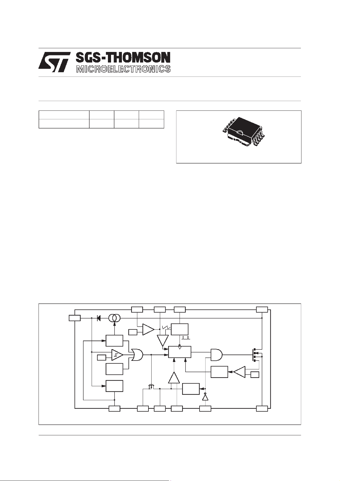
BATTERY CHARGER PRIMARY I.C.
TYPE V
DSS
VIPer31SP 600 V 1 A 6.5 Ω
I
R
n
DS(on)
VIPer31SP
ADVANCE DATA
10
FEATURE
■ RECTANGULARCHARACTERISTIC,
WITHOUT OPTOCOUPLER
■ INTERNALLY TRIMMED CURRENT
REFERENCE
■ FIXEDSWITCHING FREQUENCY,
ADJUSTABLEUP TO 150KHZ
■ AUXILIARYVOLTAGEREGULATOR
■ SOFT STARTANDSHUT DOWNCONTROL
■ AUTOMATIC BURSTMODEOPERATIONIN
STAND-BY CONDITION ABLE TO MEET
”BLUE ANGEL” NORM(<1WTOTALPOWER
CONSUMPTION)
■ UNDERVOLTAGE LOCK-OUTWITH
HYSTERESIS
■ INTEGRATED STARTUP SUPPLY
■ AVALANCHERUGGED
■ OVERVOLTAGEPROTECTION
■ OVERTEMPERATUREPROTECTION
■ CYCLEBY CYCLECURRENT LIMITATION
■ DEMAGNETISATIONCONTROL
BLOCK DIAGRAM
VCC
29 V
ON/OFF
UVLO
LOGIC
+
-
OVERTEMP.
DETECTOR
10 V
REGULATOR
2.6 V
+
1
Power SO-10
DESCRIPTION
VIPer31SP combines on the same silicon chip a
PWM control dedicated to output current
regulationtogetherwithan optimisedhighvoltage
avalanche rugged vertical power MOSFET
(600V/1A). Typical applications cover battery
chargers with constant current and constant
voltage output characteristics, without any
optocoupler between primary and secondary
sections. Typical output power capability is 15 W
in wide range condition and 30 W in single range
or with doubler configuration. Burst mode
operation is an additional feature of this device,
offering the possibility to operate in no load
condition with an input power as low as 1W. This
feature insures the compliance towards ”Blue
Angel”norm andothersimilar ones.
DRAINOSCCOMPFB
OSCILLATOR
-
+
R1
FF
R3 R4
Q
PWM
LATCH
CURRENT
REGULATION
200 ns
BLANKING
+
-
1.5 A
R2
-+
January 1998
VDD GND CREF CSENSE DSENSE SOURCE
SC12000
1/16
Page 2
VIPer31SP
ABSOLUTEMAXIMUM RATING
Symb o l Para met er Val u e Uni t
V
I
I
DREV
V
V
I
I
DSENSE
V
I
D(AV)
E
D(AV)
P
T
T
THERMALDATA
R
thj-case
R
thj-a mb.
Note 1 : This thermal resistancecorresponds to the standard mounting ona FR4 typeprinted circuit board.
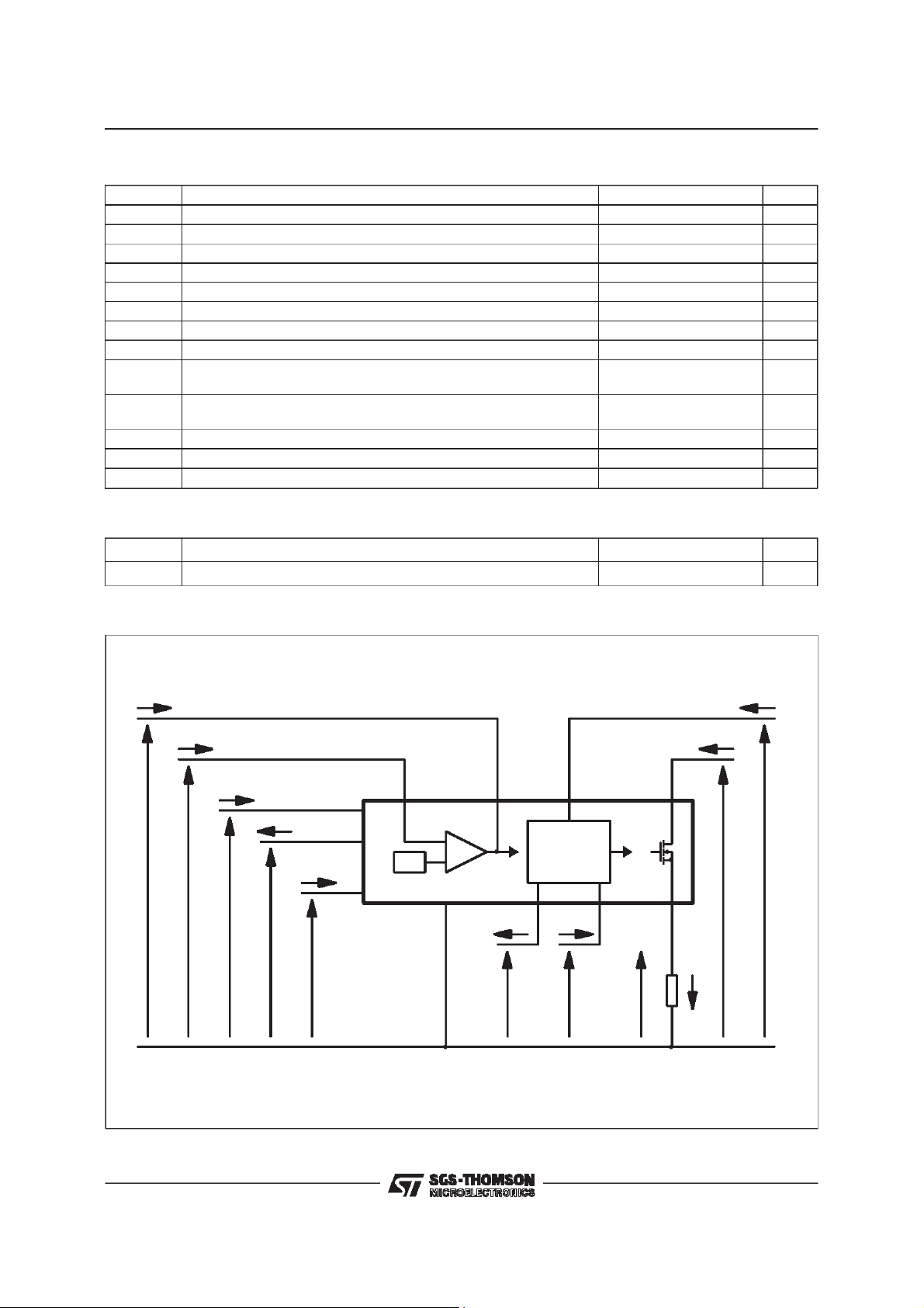
CURRENT AND VOLTAGECONVENTIONS
Continuous Dra in- Source Voltage (T j = 25 to 125oC) 600 V
DS
Maxim um DC Dra in Current Int er nall y Li mited A
D
Reverse DC Drain Current -2.5 A
Supply Volt a ge 0 to 35 V
CC
Volta ge Range Input (CS ENSE, CO MP, FB , OSC , CR E F ) -03 to V
X
Current I nput (CS ENSE, CO MP, FB, OSC, CR EF 10 mA
X
DD
Current Rang e Input (DSENS E) -10 to +10 mA
esd Elect r os ta t ic Discharge ( R = 1. 5 KΩ C=100pF)
Avalanc h e Dr ain-S o ur ce Current, Repetitive or Not-Repetit iv e
=100oC, Pulse Width Limited by TJmax)
(T
C
Avalanc h e Dr ain-S o ur ce Energy, R epetiti ve or Not - R epet i t ive
=25oC, Pulse Width Limited by TJmax)
(T
C
Power Dissipat ion at TC=25oC62W
tot
Junct ion O per at i ng Temperatur e -40 to 150
j
Stora ge Temperatu re -65 to 150
stg
2000 V
TBD A
TBD mJ
Ther mal Resist anc e Junction-cas e Max 2. 0
Ther mal Resist anc e Junction-ambient (Not e1) Max 50
o
o
o
C/W
o
C/W
V
C
C
ICOMP
IFB
ICC
6
8
2
VCC
VDD
OSC
VIPer31
2.6V
VOLTAGE CONTROL
GND
10
IDD
IOSC
VCOMP VFB VCC VDD VOSC VCREF VCSENSE VSOURCE VDRAIN VDSENSE
COMPFB
+
93
ICREF ICSENSE
111
CURRENT
CONTROL
CSENSECREF
74
DRAINDSENSE
SOURCE
5
ISOURCE
RS
IDSENSE
IDRAIN
SC12020
2/16
Page 3
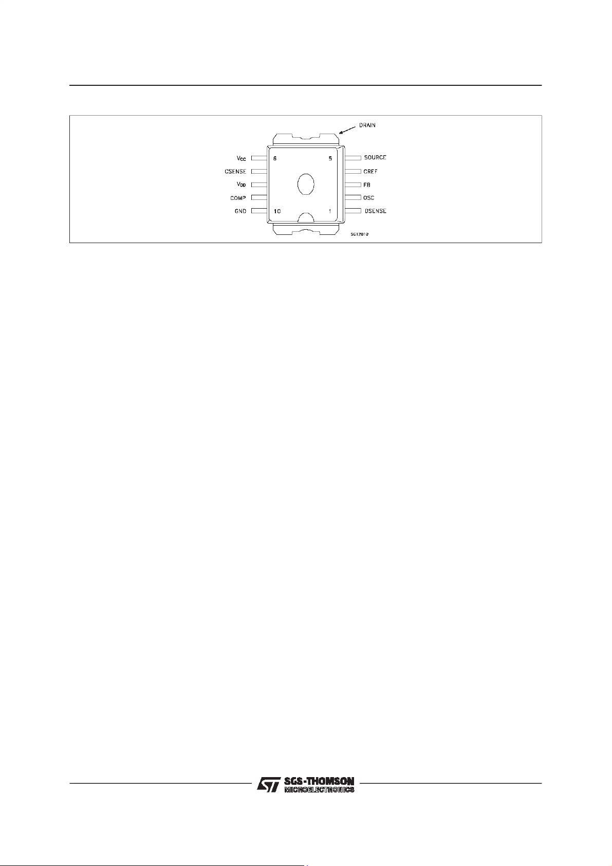
CONNECTION DIAGRAMS(top View)
VIPer31SP
PINSFUNCTIONAL DESCRIPTION
DRAINPIN:
Integrated power MOSFET drain pin. It provides
internal bias current during start-up via an
integrated high voltage current source which is
switched off during normal operation. The device
is able to handle an unclamped current during its
normal operation, assuring self protectionagainst
voltage surges, PCB stray inductance, and
allowing a snubberless operation for low output
power.
SOURCEPIN:
Integrated power MOSFET source pin. To be
connectedto an external current sense resistance
which definesthe output currentvalue.
GND
Used as the signal reference for all low level
signals. To be connected to the cold point of the
currentsenseresistance.
V
PIN:
DD
It corresponds to the low voltage supply of the
control part of the circuit. If Vdd goes below 6V,
the circuit is shut down and the start-up current
source is activated. The circuit resumes normal
operation when the V
voltage reaches 8V. An
DD
internal low drop linear regulator generates the
V
voltage from the VCCone, thus limiting its
DD
value at 10V.
PIN:
V
CC
This pin receives the auxiliary unregulated
voltage from the main transformer, which can
range from 7V up to 27V during normal operation.
It delivers a start up current of 1.5mA during the
shut down phase. The V
pin is also connected
CC
to an internal 10V low drop regulator which
providesthe V
DD
voltage.
SENSE
PIN:
C
Receives the voltage of the current sense
resistor, representativefrom the power MOSFET
drain current.
C
PIN:
REF
Serves as a reference for the peak power
MOSFETdrain current. It is also the output of the
curent regulation function, which adjusts this
reference voltage to keep the average output
current constant. To be connected to an external
filteringcapacitor.
D
SENSE
PIN:
Detects the full demagnetisation of the main
transformer, in order to drive the current
regulation function. Refer to the application part
for further details. It is also used to prevent any
new turn on of the power MOSFET during the
demagnetisationphase.
FB PIN:
This is the inverting input of the voltage mode
error amplifier. This error amplifier is in charge of
the limitation of the V
voltage when the output
CC
currentis lower than the nominal regulatedone.
COMP PIN:
This is the output of the voltage mode error
amplifier. An external R-C network connected
between this pin and the FB pin defines the
bandwidth of the voltage regulation loop, and
insures the stability ofthe converter.
OSC PIN:
An RT-CT networkmust be connected on that pin
to define the switching frequency. Note that
despite the connection of RT to V
significant frequency change occurs for V
,no
DD
DD
varying from 7V to 10V. It provides also a
synchronisationcapability, when connected to an
externalfrequencysource.
3/16
Page 4

VIPer31SP
ELECTRICAL CHARACTERISTICS (TJ=25oC, VCC= 12 V, unless otherwise specified)
POWERSECTION
Symbol Parameter Test Cond ition s Min. Typ. Max. Unit
BV
I
DSS
R
DS(on)
C
OSS
(1) On Inductive Load,Clamped.
SUPPLY SECTION
Symbol Parameter Test Cond ition s Min. Typ. Max. Unit
I
CCch
I
CC0
I
CC1
I
CC2
V
DDo f f
V
DDo n
V
DDhyst
V
DDreg
V
I
DDsc
Drain-S o ur ce Vol ta ge ID=1mA V
DSS
Of f - State Drain Current VDS=500V V
St at i c D rain S ou r ce on
Resistance
t
Fall Time ID = 0.3 A Vin= 300 V (1)
f
ID=0.3A V
=25oC
T
J
= 100oC
T
J
= 0 V 600 V
COMP
=0V 1 mA
COMP
=0V
SENSE
250 ns
(see fig. 1)
Rise Ti me ID=0.3A Vin= 300 V ( 1 )
t
r
TBD ns
(see fig. 1)
Out put Capacitanc e VDS=25V TBD pF
St art - u p Char ging
Current
Oper at i ng Supply
Current
Oper at i ng Supply
VDD=0toV
DDon
VDS= 250 V
-1.5 mA
(see fig. 2)
FSW=0KHz
10 mA
(see fig. 2)
FSW=100KHz TBD mA
Current
Oper at i ng Supply
FSW=200KHz TBD mA
Current
Undervoltage
(see fig. 2) 6 V
Shut dow n
Undervoltage Reset (see f ig. 2) 8 V
Hyst eresis St art - up (see f ig. 2) TBD 2 V
Out put Volt age (see f ig. 2) TBD TBD V
Drop Out Volt age VCC=9V IDD=TBDmA
DO
(see fig. 2)
Short Cir cuit Current VDD=0V TBD mA
6.5
10
TBD mV
Ω
Ω
OSCILLATORSECTION
Symbol Parameter Test Cond ition s Min. Typ. Max. Unit
F
SW1
F
SW2
V
OSC HI
V
OSC LO
Os cillator Freque ncy
Init i al Acc urac y
Os cillator Freque ncy
Total Variation
=8.2K
R
T
=25oC(seefig.3)
T
J
=8.2K
R
T
V
DD
Ω
Ω
=7to10V
CT= 3300 pF
CT= 3300 pF
Os cillator Peak V ol t age (1) 6.2 V
Os cillator Valley
(1) 2. 5 V
Voltage
(1) The peak and valley voltages areused internally by the voltagemode PWM. Thesawtooth generated by the oscillator is compared to
the COMP pin voltage to limit theduty cycle of thepower mosfet switch.See block diagram on page 1.
4/16
TBD 50 TBD KHz
TBD 50 TBD KHz
Page 5

VIPer31SP
ELECTRICAL CHARACTERISTICS (continued)
ERRORAMPLIFIERSECTION
Symbol Parameter Test Cond ition s Min. Typ. Max. Unit
V
REF
∆V
GBW Unity G ain Bandwidth (see f ig. 4) 400 KHz
A
VOL
I
V
COMP LO
V
COMP HI
I
COMP LO
I
COMP HI
CURRENTREGULATIONSECTION
Symbol Parameter Test Cond ition s Min. Typ. Max. Unit
V
REG
t
V
DSENSEth
V
DSENSEc l
Reference Voltage I
Tem peraure Variat ion TB D TBD %
REF
Open Loop Volt age
=0mA TJ=25oC TBD 2.6 TBD V
COMP
(see fig. 4) TBD 5 0 dB
Gain
Input Bia s Cur re nt VFB=5V 2.5 5 µA
FB
Out put Low Lev el
Out put High Le v el
Out put Low Cur rent
=-100µAVFB=5V
I
COMP
= 100 µAVFB=0V
I
COMP
V
=5V VFB=5V 3.5 mA
COMP
1V
9V
Capabili t y
Out put High Current
V
=5V VFB=0V -3.5 mA
COMP
Capabili t y
Reference Voltage
Current Sense Delay
d
(see fig. 5) 320 350 380 mV
(See f ig 1) 350 ns
to Turn-off
Demagn et iz a t ion
(see fig. 6) 2.6 V
Detector T h re shol d
Voltage
Demagn et iz a t ion
I
DSENSE
= 10 m A (see f ig. 6) 6 V
Detector Cl am ping
Voltage
PROTECTION SECTION
Symbol Parameter Test Cond ition s Min. Typ. Max. Unit
I
Dli m
Peak Drain Cur rent
Limitati on
t
Current Limita t ion
b
Blanking Time
V
CClim
VCCOve rv oltage
Threshold
V
CChystVCC
Hyst eresis
T
Ther mal S hut do wn
SD
Tem perature
T
SDhyst
Ther mal S hut do wn
Hyst eresis
Ove rv oltage
=0 (see fig. 9)
R
S
=0 (see fig. 9)
R
S
VFB= 0 V (see fig. 7) 26 35 V
VFB= 0 V (see fig. 7) 2 V
(see fig. 8) 150
(see fig. 8) TB D
12.5A
1.2 µs
o
o
C
C
5/16
Page 6

VIPer31SP
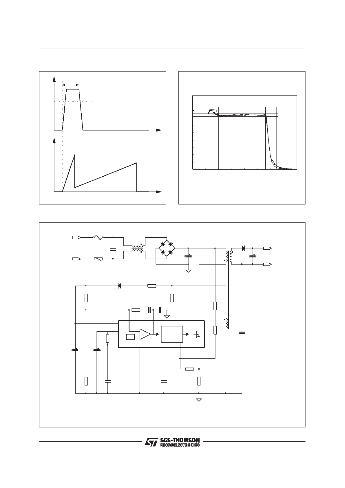
Figure 1: Switching Times
VDS
2.VIN
tf
VIN
ID
td
VCREF
RS
Figure 3: Switching FrequencySetting
Figure2: UVLO LogicBehaviour
ICC0
ICCch
ICC
VDD
VDDhyst
VDDonVDDoff
VDDreg+VDO
VCC
VCC
SC12040
Tr
t
VDDreg
t
SC12030
Oscillator frequency vs Rt and Ct
1,000
500
300
Ct= 1.5nF
200
Ct= 2.7nF
100
Ct = 4.7nF
50
Frequency (kHz)
Ct= 10nF
30
20
1 2 3 5 10 20 30 50
Rt (kΩ)
RT
OSC
CT 500
+
VDD
GND
0.62 VDD
+
+
0.25 VDD
SC12050
S
Q
R
6/16
Page 7

VIPer31SP
Figure 4: Error AmplifierPhaseand Gain
(dB) (°)
100
PHASE
50
GAIN
0
Cload = 100pF
-50
1 10 100 1k 10k 100k 1M 10M
Frequency (Hz)
200
150
100
50
0
-50
-100
-150
SC12060
Figure 5: ReferenceVoltageMeasurement
6
VCC
8
VDD
8.2k
Ω
2
OSC
VIPer31
12V
4.7uF
16V
3.3nF
COMPFB
-
2.6V
VOLTAGE CONTROL
+
GND
10
93
Vreg
111
DRAINDSENSE
CURRENT
CONTROL
74
SOURCE
5
SC12070
CSENSECREF
7/16
Page 8

VIPer31SP
Figure 6: DemagnetisationControl Logic
VDD
10µA
VDSENSEth
VDSENSEcl
GND
-
+
VAUX
AUXILIARY
WINDING
DSENSE
VCC
Figure 7: OvervoltageProtection
VCC
VCClim
VCChyst
DRAIN
FROM
PWM
LATCH
S
Q
EOD
R
1
R
D
Q
SOURCE
VDSENSEth
1
0
VAUX
t
EOD
t
SC12080
Figure8: OvertemperatureProtection
Tj
Tsd
Tsdhyst
t
VCREF
ID
SC12090
t
t
t
ID
t
VDD
VDDon
VDDoff
t
VCREF
t
SC12100
8/16
Page 9
VIPer31SP
Figure 9: Blanking Timeand Current Limitation
ID
tb
IDlim
ID
IDlim
SC12110
Figure 10: Typical AC/DCAdapter
Figure11: TypicalOutputCharacteristics
Iout vs Uout curves for Vin = 100, 200, 300, 400 VDC, Ta = 25°C
1
Iout
(A)
0.8
Constant current
t
0.6
Short circuit or
0.4
Low voltage
operation
operation (+/-2.5%)
0.2
0
51015
t
Constant voltage
operation (+/-7%)
Uout
(V)
SC12120
C7
10uF
35V
R3
27k
R10
2.7k
R1
CTN
F1
FUSE
C8
4.7uF
16V
C1
100nF
D2
1N4148
6
VCC
8
VDD
R8
2.6V
8.2k
VOLTAGECONTROL
2
OSC
U1
VIPer31
C9
2.7nF
T1
R2
22
R6
C5
10k
2.2nC41nF
93
COMPFB
+
GND
10
BR1
-+
1A/600V
R4
22k
111
CURRENT
CONTROL
CSENSECREF
C10
470nF
74
SOURCE
R9
470
10uF
400V
DRAINDSENSE
5
D1
STPS1100U
T2C2
R5
680k
R7
680k
R11
1.3
C6
2.2nF
C3
330uF
25V
IOUT
GND
L
N
SC12130
9/16
Page 10

VIPer31SP
OPERATIONDESCRIPTION:
This device is intended to be used in off line
AC/DC adapter where the desired output
characteristic must present a rectangular
characteristic. For output voltage values lower
than a fixed value, the average output current
must be constant, whatever are the input or
output voltages. If the output current consumed
by the load is lower than the previous constant
current value, the output voltage value must be
limited. In addition,the device provides protection
against output short circuits and overtemperature
events.
The two modes of operation are described in the
following paragraphs.Figure10 presentsa typical
application of which the output characteristic can
be seen on figure11.
CONSTANTOUTPUT CURRENT
The powertopology to beused with this device is
a simple discontinuous flyback, as shown on
figure 10. The average output current of such a
topology cannot be easily kept constant, as it
depends on the output voltage. Actually, if the
peak primary current is fixed, the converter
behavesas a constantpower generator.
Therefore, a modulation of the peak primary
current versus output voltage must be done in
order to get the constant output current
characteristic. A conventionalway consists to use
an optocoupler between primary and secondary,
with additional circuitry on secondary side
(Reference, error amplifier and current sense
resistor).
This device avoids the use of all the secondary
circuitry by controlling from primary side the
secondary average output current. Figure 12
presents the internal constitution of the current
control function. It is built around a constant
current source Iref, and a mosfet switch driven
with the complementedsignal EOD,in serieswith
a resistance R. The middle point of these
elements isavailable on the CREF pin.
The EOD signal is generated by the
demagnetisationfunction,which is monitoringthe
voltage of the main transformer auxiliary winding.
Figure 12: ConstantCurrentOperation
D2
R1
VCC DSENSE DRAIN
EOD
-
+
PWM
Latch
VIPer31
R2
OscillatorDemag.
Iref
C2
Uc
R
Ic
C
+Vin
Ip
Q
R
SOURCECSENSECREF GND
RS
D1
n
Is
VCREF
T
VCREF
n.
Iref-
RS
RS
EOD
Iref
IOUT
C1
GND
Ip
Is
1
0
Ic
Uc
R
Tsw
t
t
t
tonsec
t
SC12140
10/16
Page 11

VIPer31SP
An external resistance R1is needed to withstand
the negativevoltage generatedby thewinding. As
long as the transformerisdelivering some energy
on secondary side, the negated EOD signal
remains in the high stateand themosfetswitch Q
is on. The duration of this state is noted tonsec
and correspondsto the timewhere the secondary
current is flowing through D
. For details about
1
the demagnetisationfunction,refer to figure6.
The averageoutputcurrent can be expressedas:
I
t
S
I
OUT
=
ONSEC
X
2
T
SW
(1)
Where :
I
is the peak secondarycurrent.
S
t
ONSEC
T
is the conduction timeon secondary side.
isthe switching period.
SW
Taking into account the transformer ratio n
I
between primary and secondaryside,
be expressed versusprimary peakcurrent
I
=
nx
S
I
P
canalso
S
(2)
I
:
P
The value of the capacitorC is sufficientlyhigh to
consider the voltage Uc as constant. This
capacitor is submitted to a charging current and
dischargingcurrent at the rhythm of the switching
frequency. As these currents are in the range of a
few mA (Iref is typically 1 mA), a 470 nF is a
suited value for a switching frequency of 60 kHz.
In steadystate,it can be writtenthat the charge is
equal to thedischarge :
U
I
REF
x(T
SW
−
t
ONSEC
)=(
R
C
−
I
)
xt
REF
ONSEC
It comes:
T
U
As
=
R
C
xI
REF
U
can be consideredas a constant voltage,
C
x
SW
t
ONSEC
(3)
can be alsoexpressedas :
U
I
C
=
P
R
S
(4)
Combining(1),(2), (3) and (4) :
I
OUT
n
=
x
2
REF
R
S
RxI
This last expression shows that the average
output current doesn’t depend any more neither
on the output voltage, nor on the duty cycle, nor
on the input voltage. The only parameters which
are settingits valueare:
The transformerratio n.
The senseresistor value
R
S
The product
RxI
REF
This product corresponds to a voltage which is
noted Vreg in the specification tables. Figure 5
shows the test fixture for measuring it : The
DSENSEpin is held in the high state (In fact, it is
left open, as an internal pull up current source is
internally connected on this pin) and the mosfet
switch Q is always in the high state. In this case,
the voltage on the CREF pin establishes at
RxI
REF
.
Note that the oscillator must be running for the
demagnetisation block to sample correctly the
DSENSEpin.
As V
has a typicalvalue of 350 mV, the output
reg
currentcan be finallywritten as :
I
OUT
=
nx
0.175
R
S
A sense resistor of 1.3 Ω with a transformer ratio
of 6 gives a typical output current of about 800
mA.
The schematics of figure 10 shows a
compensation on the CSENSE pin with the two
resistances R5 and R7. These resistances are
connected on the Vin input voltage and are
providing an offset on the current sense pin. The
higher is the input voltage, and the higher is this
offset current. The purpose of this compensation
is to cancel the effect of the current control
propagation time td, which induces an extra
current on top of the theoretical peak current Ip
given by (4).
The output current obtained with this
compensation can be seen on figure 11. The
typical ”flatness” is about +/-2.5 %, including the
input voltagevariation from 100 VDCto 400 VDC.
If less accuracy is needed, these two resistances
can be omitted.
CONSTANT VOLTAGEOPERATION
An another part of the circuit is in charge of the
regulation of the output voltage, and generates
the vertical characteristic of figure 11. It consists
of a primary feedback regulation, with a
conventional voltage mode control : An
operational amplifier with an internal voltage
reference of 2.6 V is configured in error amplifier
and defines the duty cycle of the power mosfet
switch by comparison with the oscillator sawtooth
(Seeblock diagramon page 1).
As it is a primary feedback, the accuracy of the
output voltage depends closely on the
transformer coupling quality. This is especially
11/16
Page 12

VIPer31SP
true for low output current where the output
voltage can reach high values, as shown on
figure 11 : 20 V can be reached for a nominal
regulated one of 14.5 V, with a typical
transformer. But a simple clamping zener can
limit it to about 17 V with a reasonabledissipated
power. The 10 % to 100 % output load regulation
is betterthan +/-7 %.
COMPONENTS SIZING
The following procedure defines the value of
essential parameters for the transformer and the
sensing resistance in a typical application. The
user can adapt by himself the final design,
accordingto specificneeds,if any.
- 1. Define the maximum output voltage
MAX
V
for which the converter has still to
OUT
operatein constant currentmode.
- 2. Check that the ratio between the minimum
MIN
operating output voltage
V
OUT
lower than 2.5. This ratio is limited by the
overvoltage protection value (Typically 29 V)
and V
DDreg
(Typically 10 V) and their
tolerances.
and
V
MAX
OUT
is
- 3. Compute the transformer turn ratio n from
primaryto secondary with the formula :
100
n
=
MAX
V
OUT
n
p
=
n
s
- 4.Compute the sense resistance value with the
formula:
R
=
S
- 5. Compute the transformer turn ratio n
0.175
n
x
I
OUT
AUX
fromauxiliaryto secondary withthe formula :
n
AUX
25
=
MAX
V
OUT
n
a
=
n
s
- 6. The current control function requires the
converter to work in discontinuous mode. The
primary inductance value L
can be computed by respecting this constraint
in all conditions, or by using the following
MIN
V
formula:
MIN
V
is the minimum input rectifiedDC voltage
IN
n
L
=
P
10
IN
x
fromthe mains.
of the transformer
P
T
x
SW
I
OUT
where :
T
is the switching period.
SW
START UP SEQUENCE
An integrated high voltage current source
providesa biascurrent from the DRAIN pin during
the start-up phase. This current is partially
absorbed by internal control circuits which are
placed into a standby mode with reduced
consumption and also provided to the external
capacitorsconnectedto the V
andVCCpins.As
DD
soon as the voltage on this pin reaches the high
voltage threshold V
of the UVLO logic, the
DDon
device turns into active mode and starts
switching. The start up current generator is
switched off, and the converter should normally
provide the needed current on the VDD pin
through the auxiliary winding of the transformer,
as shown on figure 13.
The sum of the external capacitors C
and VCCpins mustbe sized according to the
V
DD
START
on the
time needed by the converter to start up, when
the device starts switching. This time t
depends
SS
on many parameters, among which transformer
design, output capacitors, capacitor value
implemented on the CREF pin (See soft start
consideration here after). The following formula
can be used for defining the minimum capacitor
needed :
IDDx
t
C
I
DD
>
START
is the consumption current on the VDDpin
when switching. Refer to specified I
V
DDhyst
SS
where :
DD1
and I
DD2
values.
t
is the start up time of the converter when the
SS
device begins to switch. Worst case is generally
at full load.
V
DDhyst
is the voltage hysteresis of the UVLO
logic. Referto theminimum specifiedvalue.
C
START
capacitorson V
allot a standard 4.7 µF / 16 V on the V
the rest on the V
=C
+C
VDD
and VCCpins.Once is defined,
DD
CC
is the sum of both
VCC
pin. The VDDcapacitor
DD
pin,and
insures a correct decouplingof the internal serial
regulatorbetweenV
and VDD.
CC
Soft start feature is implemented through the
CREF capacitor which is also filtering the CREF
voltage. The minimum value of this capacitor has
to be set accordingto the switching frequency, in
order to filter the charginganddischarging current
issued from the CREF pin (Refer to the current
control description part). Itcan be increasedfrom
12/16
Page 13

Figure 13: Start Up Circuit and Sequence
VIPer31SP
AUXILIARY
WINDING
C
VCC
VCC
LDO
Reg.
VDD
C
VDD
2mA
ON/OFF
UVLO LOGIC
Ref
VIPer31
-
+
DRAIN
SOURCEGND
this value to provide a soft start feature, of which
the durationdependson some circuitparameters,
like transformer ratio, sense resistor, output
capacitors and load. The user will define the best
appropriatevalueby experiments.
SHORT CIRCUITOPERATION
In case of abnormal condition where the auxiliary
winding is unable to provide the low voltage
supply current to the V
pin (i.e. short circuit on
CC
the output of the converter), the external
capacitors discharge themselves down to the low
threshold voltage V
off of the UVLO logic, and
DD
the deviceget back tothe inactive state where the
internal circuits are in standby mode and the start
up current source is activated. The converter
enters a endless start up cycle, with a start-up
(V)
VDDreg
VDDon
VDDoff
tss
VCC
VDD
t
SC12150
duty cycle defined by the ratioof chargingcurrent
towards discharging when the VIPer31 tries to
start. This ratio is fixed by design to 1.5 to 12,
which gives a 11% start up duty cycle, while the
power dissipation at start up is approximately0.6
W, fora 230 Vrms input voltage.
The average output short circuit current is the
product of the start up duty cycle by the output
current flowing during the active phase of the
device (See figure 14). This output current is
limited by either the CREF pin voltage, or the
internal current limitation of 1.3 A. These values
together with the low value of start-up duty cycle
prevents the stress of the output rectifiers and of
the transformerwheninshort circuit.
Figure 14 : Short circuitoperation
VDDon
VDDoff
Isc
VDD
Iout
Average
output current
t
t
SC12160
13/16
Page 14

VIPer31SP
OVERVOLTAGEPROTECTION
If the output voltage accuracy is not a concern,
but only a limitation is desired, the internal
overvoltage protection can be used. In this case,
five components can be taken out from the
schematics of figure 10 (R3-R10-R6-C4-C5) and
the input pin FB of the error amplifier is simply
grounded. The internal overvoltage protection will
act as soon as the V
voltage reaches typically
CC
29 V, by turning off the power mosfet switch. An
hysteresis of about 3 V will enable again the
switchingof the device at a lower voltagelevel on
the V
pin. This results in an efficient voltage
CC
limitation, in a burst mode operation type, with
some ripple on the output. Case by case
experimentswill define the correct value ofoutput
capacitor C3, according to the loading current in
low outputpower condition.
STANDBYMODE
The standby mode is represented by a very low
output current, corresponding to a full loaded
battery in a battery charger application. The
output voltage is limited by either the overvoltage
protection or the error amplifier, according to the
design.Thisresultsintodifferentsituations:
- In case the overvoltage protection is used, the
burst mode operation as described previously
takes place, governed by the hysteresis of the
overvoltagecomparator.
- If the erroramplifier is used,many situationcan
occur,dependingon the compensationnetwork
foreseen by the designer.These situationscan
range from a normal continuous operation, to
burst mode. In any case,the output voltage will
be regulatedto thedesired value.
Note that the burst operation is providing a very
low inputpowerconsumption,becauseit reduces
the switching frequency, and thus commutation
losses. Less than 1 W of input power can be
observed in this operative mode, with a few
hundreds of mW delivered to the secondary load.
This is far compliant with standby standards, like
the ”BlueAngel” one.
14/16
Page 15

PowerSO-10 MECHANICAL DATA
VIPer31SP
DIM.
mm inch
MIN. TYP. MAX. MIN. TYP. MAX.
A 3.35 3.65 0.132 0.144
A1 0.00 0.10 0.000 0.004
B 0.40 0.60 0.016 0.024
c 0.35 0.55 0.013 0.022
D 9.40 9.60 0.370 0.378
D1 7.40 7.60 0.291 0.300
E 9.30 9.50 0.366 0.374
E1 7.20 7.40 0.283 0.291
E2 7.20 7.60 0.283 0.300
E3 6.10 6.35 0.240 0.250
E4 5.90 6.10 0.232 0.240
e 1.27 0.050
F 1.25 1.35 0.049 0.053
H 13.80 14.40 0.543 0.567
h 0.50 0.002
L 1.20 1.80 0.047 0.071
q 1.70 0.067
α 0
o
o
8
==
==
HE
h
A
F
A1
610
51
eB
M
0.25
D
==
D1
==
E2
==
DETAIL”A”
DETAIL”A”
Q
B
0.10 A
E1E3
==
SEATING
PLANE
A
C
α
B
E4
==
SEATING
PLANE
A1
L
==
0068039-C
15/16
Page 16

VIPer31SP
Information furnished is believed tobeaccurate and reliable. However, SGS-THOMSON Microelectronics assumes no responsability for the
consequences of use of such information nor for any infringementof patents or other rightsof third parties which may resultsfrom its use. No
license is grantedby implication or otherwise underany patent orpatent rights ofSGS-THOMSON Microelectronics. Specifications mentioned
in this publication are subject to change without notice. This publicationsupersedes and replaces all information previously supplied.
SGS-THOMSON Microelectronicsproducts arenot authorizedfor useas criticalcomponents in lifesupport devicesor systems withoutexpress
written approval of SGS-THOMSON Microelectonics.
1998 SGS-THOMSON Microelectronics - Printed in Italy -All RightsReserved
Australia - Brazil - Canada - China - France - Germany - Italy - Japan - Korea- Malaysia - Malta - Morocco - The Netherlands -
Singapore - Spain - Sweden - Switzerland - Taiwan -Thailand - United Kingdom -U.S.A
16/16
SGS-THOMSON MicroelectronicsGROUP OF COMPANIES
...
 Loading...