

Page 1
HCMOS MULTI-FUNCTION PERIPHERAL
The TS68HC901 CMFP (CMOS Multi-Function
Peripheral) is acombination of many ofthe necessary peripheral functions in a microprocessor system.
Includedare :
.8 INPUT/OUTPUTPINS
• Individually programmable direction
• Individual interrupt sourcecapability
Programmable edgeselection
-
.16 SOURCEINTERRUPT CONTROLLER
• 8 Internalsources
• 8 Externalsources
• Individual source enable
• Individual source masking
• Programmable interrupt servicemodes
Polling
-
Vector generation
-
OptionalIn-servicestatus
-
• Daisy chaining capability
.FOUR TIMERS WITHINDIVIDUALLY
PROGRAMMABLE PRESCALING
• Two multimodetimers
Delay mode
-
Pulse widthmeasurement mode
-
Event counter mode
-
• Two delaymode timers
• Independent clock input
• Time outoutput option
.SINGLECHANNEL USART
• Full Duplex
• Asynchronous to65 kbps
• Bytesynchronous to1 Mbps
• Internal/External baud rate generation
• DMA handshake signals
• Modem control
• Loop backmode
.68000 BUSCOMPATIBLE
TS68HC901
48
PDIP48
1
PLCC52
(Ordering Information at the end of the Datasheet
DESCRIPTI ON
The use of the CMFP in a system can significantly
reduce chip count, thereby reducing system cost.
TheCMFPis completely68000bus compatible,and
24 directly addressable internal registers provide
thenecessary control andstatus interfacetotheprogrammer.
TheCMFP isa derivative of theMK3801 STI, aZ80
familyperipheral.
September1992
1/42
Page 2
TS68HC901
INTRODUCTION
The TS68HC901 multi-function peripheral (CMFP)
is a member of the 68000 peripherals. The CMFP
directly interfaces to the 68000processor via anasynchronous bus structure. Bothvectored and polledinterrupt schemes are supported,withtheCMFP
providing unique vectornumber generation for each
of its 16 interrupt sources. Additionally, handshake
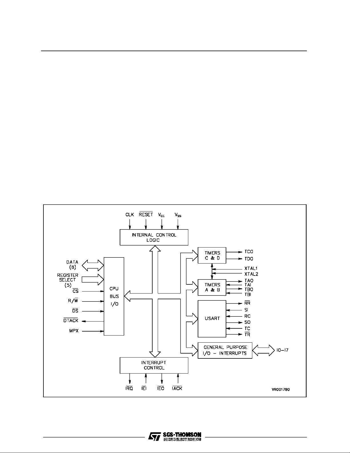
linesareprovided tofacilitate DMAC interfacing. Referto blockdiagram of the TS68HC901.
The TS68HC901 performs many of the functions
commonto most microprocessor-based systems.
The resources available to the userinclude:
.EightIndividually Programmable I/OPins withIn-
terrupt Capability
.16-Source Interrupt Controller with Individual
Source Enabling andMasking
.Four Timers, Two of which are Multi-Mode Ti-
mers
Figure 1: TS68HC901 Block Diagram
.Timers may be used as Baud Rate Generators
for the Serial Channel
.Single-Channel Full-Duplex Universal Synchro-
nous / Asynchronous Receiver-Transmitter (USART) thatSupports Asynchronous andwiththe
Addition of a Polynomial Generator Checker
Supports Byte Synchronous Formats
Byincorporating multiple functions withintheCMFP,
the systemdesigner retains flexibility while minimizing device count.
Froma programmer’s pointof view, theversatility of
the CMFPmay be attributed to its register set. The
registers arewell organized andallowthe CMFP to
be easily tailored to a varietyof applications. All of
the 24registers arealso directly addressable which
simplifies programming. The registermap is shown
in Figure2.
2/42
Page 3

Address
Binary
Hex
RS5 RS4 RS3 RS2 RS1
TS68HC901
Figure 2 : CMFP Register Map.
Abbreviation Register Name
01
03
05
07
09
0B
0D
0F
11
13
15
17
19
1B
1D
1F
21
23
25
27
29
2B
2D
2F
Note : Hex addresses assume t hat R S1 connects wit h A 1, R S2connects with A2, et c... and t hat DS is connected to LDS on
the 68000 or D S i s connec t to DS on th e 68008.
0
1
0
0
0
0
0
1
0
0
0
1
1
0
0
0
0
0
1
0
0
1
0
1
0
0
0
1
1
0
0
1
1
1
0
0
0
0
0
1
0
1
0
0
1
0
0
1
0
1
0
1
1
0
1
0
0
0
1
1
0
1
0
1
1
0
0
1
1
1
0
1
1
1
1
0
0
0
0
0
1
1
0
0
0
1
0
1
0
0
1
1
1
0
0
1
0
0
1
0
1
1
0
1
0
1
0
1
1
0
1
1
1
1
0
1
0
0
0
0
GPIP
AER
DDR
IERA
IERB
IPRA
IPRB
ISRA
ISRB
IMRA
IMRB
VR
TACR
TBCR
TCDCR
TADR
TBDR
TCDR
TDDR
SCR
UCR
RSR
TSR
UDR
General Purpose I/O Register
Active Edge Register
Data DirectionRegister
Interrupt EnableRegister A
Interrupt EnableRegister B
Interrupt Pending Register A
Interrupt Pending Register B
Interrupt In-serviceRegister A
Interrupt In-serviceRegister B
Interrupt Mask Register A
Interrupt Mask Register B
Vector Register
Timer A Control Register
Timer B Control Register
Timers C and D Control Register
Timer A Data Register
Timer B Data Register
Timer C Data Register
Timer D Data Register
Synchronous Character Register
USART Control Register
Receiver Status Register
Transmitter StatusRegister
USART Data Register
3/42
Page 4

TS68HC901
Figure 3 : PDIP Pin connection
Figure 4 : PLCC Pin connection
Pin MOTOROLA
6800 Type
MOTOROLA
Multiplexed
INTEL
PIN DESCR IPTIO N
GND : Ground
VCC: +5 volts(± 5%)
R/W : Read/Write (input). This input defines a
data transfert as a Read (High) or Write
(Low) cycle. This signal is used as WR
with an Intelprocessortype.
DTACK : This outputsignals the completion ofthe
operation phaseofa buscycleto theprocessor. If the bus cycle is a processor
read, the CMFP asserts DTACKto indicate thatthe information ontheData bus
is valid.If the buscycle is a processor to
the CMFP, DTACK acknowledges the
acceptance of the data by the CMFP.
DTACKwillbeassertedonlybyanCMFP
that has CS or IAK (and IEI) asserted.
This signal is not used with a 6800processortype.
48
47
35
CS
E
1
R/W
V
SS
CS
DS
R/W
AS
CS
RD
WR
ALE
CS : Chip Select (input, active low). CS is u-
sed to select theTS68HC901 CMFP for
accesses to the internal registers. CS
and IACK must not be asserted at the
same time.
DS : Data Stobe(input, active low).This Input
is part of the internal chip select and interrupt acknowledge functions.
The CMFP mustbe located on thelower
portionof the16-bit data-busso thatthe
vector number passed to the processor
during an interrupt acknowledge cycle
willbe located inthe low byte of the data
word.Asa result,DS mustbe connected
to the processor’s lower data strobe if
vectored interrupt are to be used. Note
thatthis forces all registers tobe located
atodd addresses and latchesdataonthe
risingedge forwrites.This signal isused
asRD with anIntel processor type.
4/42
Page 5

TS68HC901
RS1-RS5:
(A1-A5)
Register Address Bus (inputs). The address bus is used to address one of the
internal registers during a read or write
cycle.
D0-D7: Data Bus (bi-directional, tri-stateable).
This bus is usedto receive data from or
transmit data totheMFP’sinternal registers duringa processor read orwrite cycle. During an interrupt acknowledge cycle, thedata busisused to pass a vector
numberto theprocessor. Since theMFP
is an 8-bit peripheral, the MFP could be
locatedon either theupper or lowerportion of the 16-bit data bus (even or odd
address). However, during an interrupt
acknowledge cycle, the vector number
passedto theprocessor must belocated
in thelow byteof thedata word.As aresult, D0-D7 of the MFPmustbe connected to the low eightbits of theprocessor
data bus, placing MFP registers at odd
addresses if vectored interrupt are to be
used.
CLK : The clock input is a single-phase TTL
compatible signal used for internal timing . This input shouldnot begated off
at any time and must conform to minimum and maximum pulse width times.
The clock is not necessarily the system
clock in frequency nor phase. When the
bus is multiplexed (MPX=1), an address
strobe signalis connected to this pin. In
the nonmultiplexed mode (MPX=0), this
input is connected to the system clock
when used with a 68000 processor type
or to VSS(0VDC) whenused witha 6800
processor type.
RESET : Device reset. (input, active low). Reset
disables the USARTreceiver and transmitter, stops alltimers and forces the timer outputs low, disables all interrupt
channels and clears any pending interrupts.The General Purpose Interrupt/I/O
lines will be placed in the tri-state input
mode.Allinternalregisters(exceptthetimer,USART dataregisters, and transmit
status register) willbe cleared.
MPX: This inputselects thedata bus mode:
MPX =0 : non multiplexed mode
MPX=1:multiplexed mode.Theregister
select lines RS1-RS5 and the data bus
D0 -D7 are mult iplexed. An ad dress
strobemustbeconnected totheCLKpin.
IRQ : Interrupt Request (output, active low, o-
pen drain). This output signals the processor that an interrupt is pending from
the CMFP.These are 16 interrupt channels that can generate an interrupt request. Clearing the interrupt pendingregisters (IPRA and IPRB) or clearing the
inte rr u pt mask regist ers (IMRA and
IMRB)willcauseIRQ to be negated. IRQ
willalso be negated astheresultof an interrupt acknowledge cycle, unless additional interrupts are pending in t he
CMFP. Ref er t o par agraph INTE RRUPTSfor further information.
IACK : Interrupt Acknowledge (input, act ive
low). IACK is used to signal the
TS68HC901 that the CPU is acknowledging an interrupt. CS and IACk must
not beasserted atthe same time.
IEI : Interrupt Enable In (input, active low). IEI
isusedtosignalthe TS68HC901 that no
higher priority device is requesting interrupt service.
IEO : InterruptEnable Out (output, activelow).
IEO is used to signal lower priority peripherals that neitherthe TS68HC901 nor
another higher priority peripheral is requesting interrupt service.
I0-I7 : General Purpose Interrupt I/O lines.
Theselines maybe usedas interrupt inputsand/orI/Olines.Whenusedasinterrupt inputs, their activeedge isprogrammable. Adatadirection register isusedto
define which lines are to be Hi-Z inputs
and which lines are to be push-pull TTL
compatible outputs.
SO : SerialOutput.This is theoutputof the U-
SART transmitter.
SI : Serial Input. This is the input to the U-
SART receiver.
RC : Receiver Clock. This input controls the
serialbit rate of the USARTreceiver.
TC : TransmitterClock.Thisinputcontrols the
serialbit rate of the USARTtransmitter.
RR : Receiver Ready. (output, active low)
DMA output for receiver, which reflects
the status of Buffer Full in port number
15.
TR : Transmitter Ready. (output, active low)
DMA output for transmitter, which reflects the status of Buffer Empty in port
number 16.
5/42
Page 6

TS68HC901
TAO,TBO,
TCO,TDO:
Timer Outputs. Each of the four timers
has an output which can produce a
square wave. The output will change
states each timercycle; thusone fullperiod of thetimer out signal is equal to two
timer cycles. TAO or TBO can be reset
(logic ”O”)by a writeto TACR,or TBCR
respectively.
TAI,TBI: Timer A, B inputs. These inputs are
controlsignals for timers A and B in the
pulse width measurement mode and event count mode. These signals generate interrupts at the same priority level
asthegeneral purpose I/Ointerrupt lines
I4 and I3, respectively. I4 and I3 do not
haveinterrupt capability when thetimers
areoperated inthepulsewidthmeasure-
XTAL1,
XTAL2 :
Timer Clock inputs. A crystal can be
connectedbetween XTAL1 and XTAL2,
or XTAL1 can bedriven witha TTL level
clock.WhendrivingXTAL1with aTTLle-
mentmode orthe event countmode -under these conditions I4 and I3 may only
be used for I/O. Refer to paragraph TIMERSfor further information.
velclock,XTAL2 mustbeallowedtofloat.
Whenusingacrystal,external capacitors
are required. See figure 35. All chip acces s es are independent of t he tim er
clock.
SIGNAL SUMMARY.
Signal Name Mnemonic I/O Active
Power Input V
Ground GND Input Low
Clock CLK Input N/A
Chip Select CS Input Low
Data Strobe DS Input Low
Read/Write R/W Input Read-High / Write-Low
Data tranfer Acknowledge DTACK Output Low
Register Select Bus RS1-RS5 Input N/A
Data Bus D0-D7 I/O N/A
Reset RESET Input Low
Interrupt Request IRQ Output Low
Interrupt Acknowledge IACK Input Low
Interrupt Enable In IEI Input Low
Interrupt EnableOut IEO Output Low
General Purpose I/O - Interrupt Lines I0-I7 I/O N/A
Timer Clock XTAL1,XTAL2 Input High
Timer Inputs TAI, TBI Input N/A
Timer Outputs TAO, TBO, TCO, TDO Output N/A
Serial Input SI Input N/A
Serial Output SO Output N/A
Receiver Clock RC Input N/A
Transmitter Clock TC Input N/A
Receiver Ready RR Output Low
Transmitter Ready TR Output Low
MPX MPX Input N/A
CC
Input High
6/42
Page 7

BUSOPERATION
Thefollowingparagraphs explain the controlsignals
and bus operation during data transfer operations
andreset.
DATA TRANSFER OPERATIONS.
Transfer ofdata between devicesinvolvesthe follo-
wing pins: Register Select Bus - RS5 throughRS1
DataBus - D0 throughD7 ControlSignals The address and databusesareseparate parallel busesused to transfer data using an asynchronous bus
structure.In all cycles, thebus master assumes responsibilityfordeskewing allsignals itissuesatboth
the start and end of a cycle. Additionally, the bus
master is responsible for deskewing the acknowledge and data signalsfrom theperipheral devices.
ReadCycle. To read a CMFP register, CS andDS
must be asserted, and R/W must be high. The
CMFPwill place the content of the registerwhich is
selected by the register select bus (RS1 through
RS5) on the data bus(D1 through D7)and then assertDTACK. The register addresses are shownon
Figure2. Aftertheprocessor has latchedthedata, DS
is negated. The negation of either CSor DS will terminate the read operation. The CMFP will drive
DTACKHigh andplace itinthehigh-impedance state.
Thetimingfor areadcycleis shown in figure 21.
WriteCycle.To writea register CSand DS must be
asserted,and R/W must below. TheCMFP willdecodetheaddress bus todetermine which registeris
selected. Then the register will be loaded with the
contentsof thedata bus and DTACK will be asserted. When the processor recognizes DTACK, DS
will be negated.The write cycle is terminated when
either CS or DS is negated. The CMFP will drive
DTACKhighandplaceitinthehigh-impedance state.
Thetimingfor awritecycleisshown in figure22.
TS68HC901
INTERRUPTACKNOWLEDGE OPERATION.
The CMFP has 16 interruptsources, eight internal
and eight external. When an interrupt request is
pending,theCMFPwillassertIRQ. In a vectored interruptscheme,the processor willacknowledge the
interruptrequestbyperforming aninterrupt acknowledge cycle. IACK and DS will be asserted. The
CMFPresponds totheIACKsignalbyplacing avector number on the lower eight bits of the data bus.
This vectornumber corresponds tothe IRQhandler
for the particular interrupt requesting service. The
format ofthis vector number is given in figure6.
Whenthe CMFPasserts DTACKtoindicate that valid data isonthebus, theprocessor willlatchthe data and terminate the bus cycle by negating DS.
WheneitherDS orIACKarenegated, theCMFPwill
terminate the interrupt acknowledge operation by
driving DTACK high and placingit inthe high-impedance state. Also, thedata buswillbe placed in the
high-impedance state.IRQ will benegatedas a result of the IACK cycle unless additional interrupts
are pending.
The CMFP can be part of a daisy-chain interrupt
structurewhich allows multiple CMFPsto be placed
at the same interrupt level by sharing a common
IACK signal.A daisy-chain priority schemeisimplemented with IEI and IEO signals. IEI indicates that
no higherpriority device is requesting interrupt service. IEOsignals lowerpriority devices that neither
this devicenor any higher priority devices is requesting service. To daisy-chain CMFPs, the highest
priority CMFP has its IEI tied low and successive
CMFPs havetheirIEI connected to the next higher
priority device’sIEO.Notethatwhenthedaisy-chain
7/42
Page 8

TS68HC901
interrupt structure is notimplemented, the IEI of all
CMFPsmust betied low.
When the processor initiates an interrupt acknowledge cycle by driving IACK and DS, the CMFP
whoseIEI is low may respond witha vectornumber
if interrupt is pending. If this device doesnot have a
pending interrupt, IEO is asserted which allowsthe
nextlowerpriority device to respond to the interrupt
acknowledge. When an CMFP propagates IEO, it
willnot drive thedata bus norDTACK during the interruptacknowledge cycle. The timingfor an IACK
cycleis shown in figure 23 and 24.
RESET OPERATION
The reset operation will initialize the CMFP to a
known state. Thereset operation requires that the
RESET input be asserted for a minimum of two
microseconds. During a device reset condition, all
internal CMFP registers are cleared except for the
timer data registers (TADR, TBDR, TCDR and
TDDR), the USART data register (UDR), the transmitterstatus register (TSR) andthe interrupt vector
register. Alltimers are stopped and the USART receiver and transmitter are disabled. The interrupt
channelsare also disabled and any pending inter-
rupts are cleared. In addition, the general purpose
interruptI/Olinesare placed in thehigh-impedance
inputmode andthetimeroutputsaredrivenlow. ExternalCMFPsignalsarenegated.The interrupt vector register is initialized to a0Fh.
NON MULTIPLEXED MODE
In this mode, theMPX inputmustbe setto zero, and
the TS68HC901 can be used witha 68000 processortype or a6800processor type.Referto figure 21
to 24for the electrical characteristics.
With a6800processor typetheDS pin isconnected
to the E signal of the processor, the DTACK signal
is not usedand the CLKmust be zeroed.
MULTIPLEXED MODE
The CMFPcan beusedeitheron aMOTOROLAor
INTELbus type. Inthiscasethe MPX pinisconnected to Vcc. The table page4 givesthe signification
ofthe differentsignals used. Adummyaccessto the
TS68HC901 hasto be done beforeany validaccess
in orderto set upthe internal logicof sampling.
8/42
Page 9

TS68HC901
INTERRUPT STRUCTURE
In a 68000 system, the CMFP will be assigned to
oneof the sevenpossible interrupt levels.All interrupt service requests from the CMFP’s 16 interrupt
channelswillbepresented atthislevel.Although,as
an interrupt controller, the CMFP will internally prioritize its 16 interrupt sources. Additional interrupt
sourcesmay be placed at the same interrupt level
bydaisy-chaining multipleCMFPs.The CMFPswill
be prioritized bytheir position in the chain.
INTERRUPTPROCESSING
Each CMFP provides individual interrupt capability
for itsvarious functions. When aninterrupt isreceivedononeofthe external interrupt channels or from
oneof theeight internal sources,the CMFP willrequest interrupt service. The 16 interrupt channels
areassigneda fixedpriorityso thatmultiplepending
interrupts areservicedaccordingto theirrelativeimportance. Since the CMFP can internally generate
16vectornumbers, the unique vectornumber which
corresponds to the highest priority channel that as
apending interrupt ispresented totheprocessorduring an interrupt acknowledge cycle. This unique
vectornumber allows theprocessor to immediately
beginexecution of theinterrupt handler fortheinterrupt source,decreasing interrupt latencytime.
INTERRUPTCHANNEL PRIORITIZATION
The 16 interrupt channels are prioritized as shown
in figure5. General purpose interrupt 7(I7)is thehighest priority interrupt channel and I0 is the lowest
priority channel.Pendinginterruptsarepresented to
the CPU in order of priority unless theyhave been
masked off. By selectively masking interrupts, the
channelare in effectre-prioritized.
INTERRUPTVECTORNUMBER FORMAT
During an interrupt acknowledge cycle,a unique 8-
bit vector number is presented to the systemwhich
corresponds tothespecificinterrupt source which is
requesting service. The format of the vector is
shown in figure 6. The most significant four bits of
the interruptvectornumberareuserprogrammable.
These bits are set by writing the upper four bits of
the vector register which is shown in figure 7. The
low order bits are generated internally by the
TS68HC901. Note that the binary channel number
shown in figure 5 corresponds to the low order bits
of thevector number associated witheach channel.
Figure 9 : Interrupt Channel Prioritization
Figure 5 : Interrupt Channel Prioritization
Priority Channel Descriptio n
HIGHEST
LOWEST
1111
1110
1101
1100
1011
1010
1001
1000
0111
0110
0101
0100
0011
0010
0001
0000
General Purpose Interrupt 7(I7)
General Purpose Interrupt 6(I6)
Timer A
Receive Buffer Full
Receive Error
Transmit Buffer Empty
Transmit Error
Timer B
General Purpose Interrupt 5(I5)
General Purpose Interrupt 4(I4)
Timer C
Timer D
General Purpose Interrupt 3(I3)
General Purpose Interrupt 2(I2)
General Purpose Interrupt 1(I1)
General Purpose Interrupt 0(I0)
9/42
Page 10
TS68HC901
V7 V6 V5 V4 IV3 IV2 IV1 IV0
V7-V4 The four mostsignificant bitsare copied from the register
IV3-IV0 These bitsare supplied by the CMFP.They are thebinary channel number of the highest
priority channel that is requesting interrupt service.
Figure 6 :
Figure 7 :
VR
(17h)
7
V7 V6 V5 V4 S 0* 0* 0*
Writin g 0 : CLEARED
Writing 1 : SET
CLEARED on RESET
VECTOR REGISTER
0
V7-V4 The upper fourbitsof the vectorregister are writtenby the user. These bits become themost
significant four bits of the interrupt vector number.
S In-Service Register Enable. When the Sbit is zero,the CMFP isin the automatic end-of-in-
terrupt mode and the In-Service register bits are forced low. When the S bit is a one, the
CMFP isin the software end-of-interrupt mode and the In-Service register bits areenabled.
* Unused bits,read as zero.
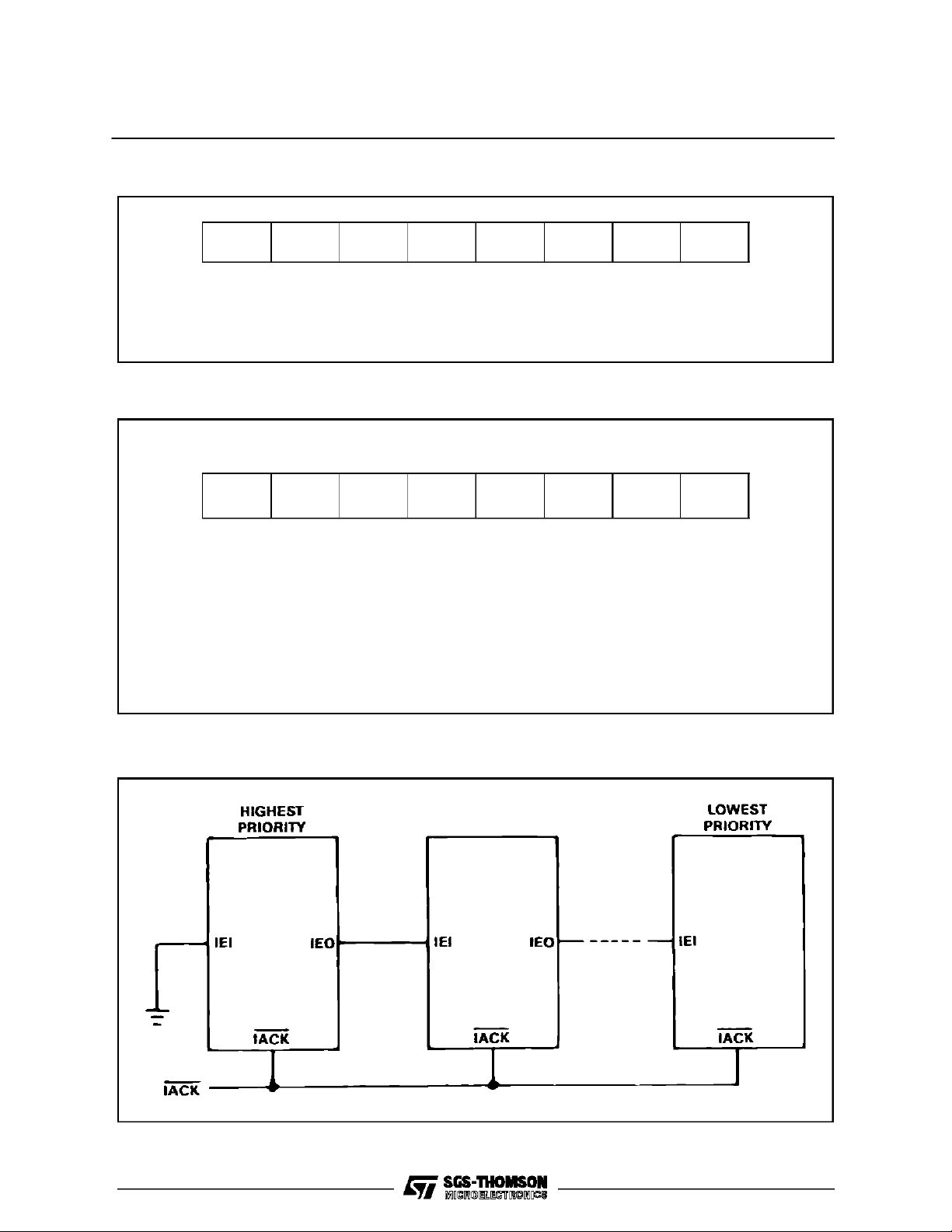
Figure 8 : Daisy Chaining
TS68HC901 TS68HC901
TS68HC901
10/42
Page 11

TS68HC901
DAISY-CHAINING CMFPs
As an interrupt controller, the TS68HC901 CMFP
willsupport eight external interrupt sources in addition to its eight internal interrupt sources. When a
system requires more than eight external interrupt
sources to be placed at the same interrupt level,
sourcesmaybe added totheprioritized structureby
daisy-chaining CMFPs. Interrupt sources areprioritized internally within each CMFP and the CMFPs
areprioritized by their position inthe chain. Unique
vector numbers are provided for each interrupt
sources.
The IEI and IEO signals implement the daisy-chainedinterrupt structure.TheIEIofthehighest priority
CMFPis tied low and the IEO output of this device
is tied to the next highest priority CMFP’s IEI. The
IEI andIEO signalsaredaisy-chainedinthismanner
for all CMFPs in the chain, with the lowest priority
CMFP’s IEO left unconnected. A diagram of an interrupt daisy-chain is shownin figure8.
Daisy-chaining requires that all parts in the chain
have a commonIACK. Whenthe common IACK is
asserted duringan interrupt acknowledge cycle, all
partswillprioritize interrupts inparallel.Whenthe IEI
signalto aCMFP is asserted, the part may respond
to the IACK cycle if it requires interrupt service.
Otherwise,the partwill assert IEO tothe next lower
priority device. Thus, priority is passed down the
chainvia IEI andIEO until a part whichhas appending interrupt isreached. Thepart with the pending
interrupt passes a vector number to the processor
and doesnot propagate IEO.
Figure 9a :
Figure 9b :
11/42
Page 12

TS68HC901
INTERRUPTCONTROL REGISTERS
CMPFinterruptprocessing ismanagedbytheinter-
rupt enable registers A andB, interrupt pending registersA andB, andinterrupt mask registers A and
B.These registers allow theprogrammer to enable
or disable individual interrupt channels, mask individual interrupt channels,and accesspending interruptstatusinformation. In-service registers Aand B
allow interrupts tobe nestedas describedhereafter.
The interrupt control registers are shown in figure10.
INTERRUPTENABLE REGISTERS
Theinterrupt channels are individually enabled ordi-
sabledby writing a one or zero,respectively, tothe
appropriate bit of interrupt enable register A(IERA)
or interrupt enable register B (IERB).Theprocessor
may readthese registers at anytime.
When a channel is enabled, interrupts received on
the channel will be recognized by the CMFP and
IRQwillbe asserted tothe processor,indicatingthat
interrupt service isrequired. On the otherhand, adisabledchannel is completely inactive; interrupts receivedon the channel are ignored by theCMFP.
Writinga zero to a bitof interrupt enable register A
orB willcausethecorresponding bitofinterrupt pendingregister A orB tobe cleared. This willterminate
allinterrupt service requests forthe channel and also negate IRQ,unless interrupts are pending from
other sources. Disabling a channel, however,does
not affect the corresponding bit in interrupt in-serviceregistersA or B. So, if theCMFPis in thesoftware end-of-interrupt mode and an interrupt is in
service whena channel will remainset until cleared
bysoftware.
INTERRUPTPENDINGREGISTERS
When aninterrupt is received onan enabled chan-
nel, the corresponding interrupt pending bitis set in
interrupt pending register A orB (IPRAor IPRB). In
a vectoredinterruptscheme, thisbit willbe cleared
when the processor acknowledges the interrupting
channeland the CMFPresponds witha vectornumber. In a polled interrupt system, the interrupt pending registers must be read to determine the interruptingchannel andthentheinterrupting pending bit
is cleared by the interrupt handling routine without
performing aninterrupt acknowledge sequence.
A singlebit of theinterrupt pending registers iscleared insoftwareby writing onesto all bitpositionsexcept thebit to be cleared. Note that writing ones to
IPRA and IPRB has no effect on the contents of the
register. A single bit of the interrupt pending registersisalsoclearedwhenthecorresponding channel
is disabled bywriting azero tothe appropriate bitof
IERA orIERB.
INTERRUPTMASK REGISTERS
Interrupts are masked for a channel by clearing the
appropriate bitin interrupt mask register Aor B(IMRA or IMRB). Even though an enabled channel is
masked, the channel will recognize subsequent interruptsand set its interrupt pending bit. However,
the channel is prevented from requesting interrupt
service(IRQ tothe processor) as long as the mask
bit forthat channel is cleared.
If achannelisrequestinginterruptserviceatthetime
that its corresponding bit in IMRA or IMRBis cleared, the request will ceaseandIRQ will benegated,
unless anotherchannel is requesting interrupt service.Later,whenthemaskbit isset,any pendinginterrupt on thechannel will be processed according
to the channel’s assigned priority. IMRAand IMRB
may be read at any time.
12/42
Page 13

TS68HC901
Figure 10 :
IERA
(07h)
IERB
(09h)
IPRA
(0Bh)
IPRB
(0Dh)
ISRA
(0Fh)
7
GPIP7 GPIP6 TIMER A
GPIP5 GPIP4 TIMER C TIMER D GPIP3 GPIP2 GPIP1 GPIP0
7
GPIP7 GPIP6 TIMER A
GPIP5 GPIP4 TIMER C TIMER D GPIP3 GPIP2 GPIP1 GPIP0
Writing0:CLEAR
Wri ting 1 : UNCHANG ED
7
GPIP7 GPIP6 TIMER A
INTERRUPT ENABLEREGISTERS
RCV
Buffer full
RCV
Error
XMIT
Buffer Empty
INTERRUPT PENDING REGISTERS
RCV
Buffer full
RCV
Error
XMIT
Buffer Empty
INTERRUPT IN-SERVICEREGISTERS
RCV
Buffer full
RCV
Error
XMIT
Buffer Empty
XMIT
Error
XMIT
Error
XMIT
Error
0
TIMER B
0
TIMER B
0
TIMER B
ISRB
(11h)
IMRA
(13h)
IMRB
(15h)
GPIP5 GPIP4 TIMER C TIMER D GPIP3 GPIP2 GPIP1 GPIP0
7
GPIP7 GPIP6 TIMER A
GPIP5 GPIP4 TIMER C TIMER D GPIP3 GPIP2 GPIP1 GPIP0
Writing 0 : MASKED
Writing 1 : UN MASKED
INTERRUPT MASK REGISTERS
RCV
Buffer full
RCV
Error
Buffer Empty
XMIT
XMIT
Error
0
TIMER B
13/42
Page 14

TS68HC901
NESTING CMFPINTERRUPTS
In a 68000vectored interrupt system,the CMFP is
assignedto one of seven possible interrupt levels.
Whenaninterrupt isreceived fromtheCMFP,aninterruptacknowledge for thatlevel is initiated. Once
an interrupt isrecognized at a particular level,interrupts at that same level or below are masked by
68000. As long as theprocessor’s interrupt mask is
unchanged, the 68000 interrupt structure will prohibitthe nesting ofinterrupts at thesame interrupt level.However,additional interrupt requests from the
CMFP can be recognized before a previous channel’s interrupt serviceroutine is completed byloweringtheprocessor’s interrupt maskto thenextlower
interrupt level within the interrupt handler.
WhennestingCMFP interrupts, it may be desirable
to permit interrupts on any CMFP channel, regardless ofits priority, topreempt ordelayinterrupt processingof an earlier channel’s interruptservice request. Or, it may be desirable to only allow subsequenthigher priority channel interrupt requests to
supersede previously recognized lower priority interruptrequests. The CMFPinterrupt structureprovides this flexibility by offering two end-of-interrupt
options for vectored interrupt schemes. Note that
theend-of-interrupt modesare not activein a polled
interrupt scheme.
SELECTING THE END-OF-INTERRUPT MODE
In a vectoredinterrupt scheme, the CMFP maybe
programmed tooperate ineitherthe automatic endof-interrupt mode or the software end-of-interrupt
mode.The mode is selected by writing the S bitof
the vectorregister (see figure7). When the S bitis
programmed to a one, the CMFP is placed in the
software end-of-interrupt mode and when the S bit
isa zero,all channels operate inthe automaticendof-interrupt mode.
AUTOMATICEND-OF-INTERRUPT
When an interrupt vector number is passed to the
processor during an interrupt acknowledge cycle,
the corresponding channel’s interrupt pending bitis
cleared. In the automatic end-of-interrupt mode, no
furtherhistoryof theinterrupt remainsin theCMFP.
The in-service bits of the interrupt in-service registers (ISRA and ISRB) are forced low. Subsequent
interrupts which arereceived onanyCMFP channel
will generate an interrupt request to the processor,
evenif the currentinterrupt’s service routine hasnot
been completed.
SOFTWAREEND-OF-INTERRUPT
In thesoftwareend-of-interrupt mode,the channel’s
associatedinterrupt pendingbitiscleared andinaddition,the channel’sin-servicebitofin-serviceregister A or B is set when its vector number is passed
to theprocessor duringanIACKcycle.A higher prioritychannelmaysubsequently requestinterrupt serviceandbe acknowledged, but as long as thechannel’s in-service bit is set, no lower priority channel
may request interrupt servicenor passitsvectorduring aninterrupt acknowledge sequence.
While onlyhigher priority channels may requestinterruptservice, any channel canreceiveaninterrupt
and set its interrupt pending bit. Even the channel
whose in-service bitis set can receivea secondinterrupt. However, no interrupt service request is
made untilits in-service bit iscleared.
The in-service bit for a particular channel can be
cleared by writing a zero to itscorresponding bit in
ISRA or ISRB and ones to all other bit positions.
Since bits in the in-service registers can only be
cleared insoftware and notset, writingones to the
register does not alter their contents. ISRA and
ISRB maybe read atany time.
14/42
Page 15

GENERALPURPOSE INPUT/OUTPUT
INTERRUPT PORT
Thegeneral purpose interrupt input/output(I/O)port
(GPIP)provides eight I/O lines (I0 through I7) that
may be operated as either inputs or outputs under
softwarecontrol.In addition, these linesmay optionally generatean interrupt oneithera positivetransition or negative transition of the input signal. The
flexibility oftheGPIPallows it tobeconfigured asan
8-Bit I/0 port or for bit I/O. Since interrupts are enabled on a bit-by-bit basis, a subset of the GPIP
could be programmed as handshake lines or the
port could be connected to as many aseight external interrupt sources, which wouldbe prioritized by
theCMFP interrupt controllerfor interruptservice.
6800 INTERRUPTCONTROLLER
The CMFP interrupt controller is particularly useful
ina system whichhasmany 6800-type devices. Typically, in a vectored 68000 system,6800-type peripherals use the autovector which corresponds to
their assigned interrupt level since they do notprovide a vector number in response to an AC cycle.
The autovector interrupt handler must then poll all
6800-type devices at that interrupt level to determine whichdevice is requesting service.However,
bytying the IRQoutput from a6800-type device to
the general purpose I/O interrupt port (GPIP) of a
CMFP,a unique vector number will be provided to
the processor during an interrupt acknowledge cycle. Thisinterrupt structure will significantly reduce
interrupt latencyfor6800-typedevicesandotherperipheral devices which do notsupport vector-by-device.
TS68HC901
GPIPCONTROL REGISTERS
The GPIPis programmed viathree control registers
shown in figure 11. These registers control thedata
directionprovideuseraccessto theport,andspecify
the active edge for each bit of the GPIP whichwill
produce an interrupt.Theseregisters are described
in detail in thefollowing paragraphs.
GPIPDATA REGISTER
The general purpose I/O dataregister is used to in-
put or outputdata to the port.When data is written
to the GPIP data register, those pins which aredefined as inputs will remain in the high-impedance
state.Pins which are defined asoutputs willassume
the state (high or low) of their corresponding bit in
the data register. Whenthe GPIP is read, data will
be passeddirectlyfrom the bitsof thedata register
forpinswhicharedefinedasoutputs. Datafrompins
defined asinputs will come from the inputbuffers.
ACTIVEEDGE REGISTER
The active edge register (AER) allows each of the
GPIP lines to produce an interrupt on either a oneto-zeroorazero-to-one transition. Writing azerothe
appropriate edge bit of the active edge register
causesthe associatedinputtogeneratean interrupt
on the one-to-zero transition. Writing a one to the
edge bitwillproducean interrupt onthe zero-to-one
transitionof the corresponding GPIPline.
15/42
Page 16

TS68HC901
Figure 11 :
7 ACTIVE EDGE REGISTER
AER
(03h)
DDR
(05h)
GPIP
(01h)
GPIP7 GPIP6 GPIP5 GPIP4 GPIP3 GPIP2 GPIP1 GPIP0
DATA DIRECTION REGISTER
GPIP7 GPIP6 GPIP5 GPIP4 GPIP3 GPIP2 GPIP1 GPIP0
GENERAL PURPOSE I/O DATA REGISTER
GPIP7 GPIP6 GPIP5 GPIP4 GPIP3 GPIP2 GPIP1 GPIP0
Note
The transition detector is an exclusive-OR gate
whoseinputs are the edgebit and theinput buffer.
Asaresult,writing the EAR maycause an interruptproducing transition, depending upon the state of
theinput. So,the AER should beconfigured before
enabling interrupts viathe interrupt enable registers
(IERA and IERB). Also, changing the edge bitwhile
interrupts are enabled maycauseaninterrupton the
corresponding channel.
0
1 = RISING
2 = FALLING
1 = OUTPUT
2 = INPUT
DATA DIRECTIONREGISTER
The data direction register (DDR) allows the pro-
grammer to define I0 through I7as inputsoroutputs
by writing the corresponding bit. When a bit of the
data direction registeris written as a zero, the corresponding interrupt I/O pin will be a high-impedance input.Writing a one to anybit of the datadirectionregister will causethe corresponding pin to
be configured as a push-pull output.
16/42
Page 17

TS68HC901
TIMERS
The CMFP contains four 8-bit timers whichprovide
manyfunctionstypically required inmicroprocessor
systems.Thetimerscansupplythe baudrateclocks
forthe on-chip serial I/O channel, generate periodic
interrupts, measureelapsed time,and count signal
transitions. In addition, two timers have waveform
generation capability.
All timers are prescaler/counter timers with a
common independent clock input (XTAL1 or
XTAL2)andarenot required tobeoperated fromthe
system clock. Each timer’s output signal toggles
whenthetimer’s main counter timesout.Additionally, timers A and B have auxiliary control signals
which are used in two of the operation modes. An
interrupt channel is assigned to each timer and
whenthe auxiliary control signals areused,a separate interrupt channel will respond totransitions on
these inputs.
OPERATION MODES
TimersA andB arefullfunction timers which, in ad-
dition tothe delay mode,operate in the pulse width
measurement mode andthe eventcountmode. TimersC and D are delay timers only. A brief discussionof each ofthe timermodes follows.
DELAY MODEOPERATION
All timers may operate in the delay mode. In this
mode,the prescaler isalways active.The prescaler
specifies the number of timer clock cycles which
must elapse before a count pulse is applied to the
maincounter. A countpulsecauses the main counterto decrement by one. Whenthe timerhasdecremented down to 01 (hexadecimal), the next count
pulse will cause the main counter to be reloaded
fromthe timer dataregister and a time out pulse will
be produced. This time out pulseis coupled to the
timer’s interrupt channel and, if the channel is enabled,aninterrupt willoccur. Thetimeoutpulsealso
causesthe timeroutput pin totoggle. The output will
remainin this newstate until the next timeoutpulse
occurs.
Forexample, ifdelaymodewithadivide-by-10 prescalerisselected and thetimerdataregister isloaded
with 100 (decimal), themaincounterwilldecrement
once every10 timer clockcycles. After 1,000 timer
clocks,a time outpulse will be produced. This time
out pulse will generate aninterrupt if the channel is
enabled (IERA, IERB) and in addition, the timer’s
output linewill toggle. The outputline will complete
onefull period every2,000 cycles ofthe timer clock.
If the prescaler value is changed while the timer is
enabled, thefirst time out pulse will occur at anindeterminate time no less than one nor more than
200 timer clock cycles.Subsequent timeout pulses
will thenoccur atthe correctinterval.
If themaincounter is loaded with 01(hexadecimal),
a time out pulse willoccur everytime the prescaler
presents a count pulse to the main counter. If the
main counter isloaded with 00, atime out pulse will
occur every 256 count pulses.
PULSE WIDTH MEASUREMENT OPERATION
Besidesthedelaymode,timersAand Bmaybepro-
grammed to operate in the pulse width measurement mode. In this mode an auxiliary control input
is required ; timersA and B auxiliary inputlines are
TAI and TBI. Also, inthe pulse widthmeasurement
mode, interruptchannels normally associated with
I4 and I3will respond to transitions on TAI andTBI,
respectively. General purpose lines I3 and I4 may
stillbeusedforI/O. Aconceptual circuitofthe timers
17/42
Page 18

TS68HC901
Figure 12 :
in the pulse width measurement mode is shown in
Figure 12.
Thepulse width measurementmode functionssimilarlyto the delay mode,with theauxiliary controlsignal acting as an enable to the timer. When the
controlsignal isactive,theprescaler andmaincounter areallowed to operate. When thecontrol signal
isnegated, thetimeris stopped.So, the widthofthe
activepulse onTAI orTBI ismeasured bythe numberof timer countswhich occur whilethetimerisallowedto operate.
The active stateof the auxiliaryinput lineis defined
bythe associated interrupt channel’s edge bit in the
activeedgeregister (AER). GPIP4 oftheAER isthe
edge bit associated withTAI and GPIP3is associatedwith TBI.Whentheedge bit isa one, theauxiliary
input will be active high,enabling the timer while the
input signal is at a high level.If the edge bit is low,
theauxiliary inputwillbe activelowandthe timer will
operate while the inputsignal isat a lowlevel.
The state of the active edge bitalso specifies whether a zero-to-one transition or a one-to-zero transitionoftheauxiliaryinputpinwillproduceaninterrupt
whenthe interrupt channel is enabled. In normaloperation, programming the activeedge bit toa one
will produce an interrupt on the zero-to-one transitionof theassociatedinput signal. Alternately, pro-
gramming theedge bitto a zero willproduce aninterrupt on the one-to-zero transition of the input signal. However, in the pulse width measurement
mode, theinterrupt generated bya transition on TAI
or TBI will occur on the opposite transition as that
normally defined bythe edgebit.
For example, in the pulse width measurement
mode, ifthe edge bit is aone, the timerwillbe allowed torunwhiletheauxiliaryinputTAIishigh.When
TAI transitions from high to low, the timer will stop
and, if the interrupt channel is enabled, an interrupt
will occur. Byhaving the interrupt occur on the oneto-zero transition instead of the zero-to-one transition, the processor will be interrupted when the
pulsebeingmeasured has terminatedandthe width
of the pulse is available from the timer. Therefore,
the timersact like a divide-by-prescaler that canbe
programmed by the timer data register and the timer’s A and Bcontrol register.
After reading the contents of the timer, the main
counter must be reinitialized by writing to the timer
dataregister toallow consecutivepulsesto bemeasured. If thetimer is written after the auxiliary input
signalis active,thetimerwillcount from the previous
contents of the timer data register until it counts
through 01 (hexadecimal). At the time, the main
counter isloaded with thevaluefrom thetimer data
register, atimeoutpulseisgenerated whichwilltog-
18/42
Page 19

TS68HC901
gle the timer output, and aninterrupt may be optionally generated on the timerinterruptchannel.
Note that the pulse width measured will include
countsfrom before the main counter was reloaded.
If thetimer data register iswritten while the pulse is
transitioningto theactivestate,an indeterminate value may be written intothe main counter.
Oncethe timeris reprogrammed foranother mode,
interrupts willagainoccurasnormally definedbythe
edgebit.Note that aninterrupt maybe generated as
the result of placing the timer into the pulse width
measurement mode orby reprogramming the timer
for another mode. Also, an interruptmaybe generated bychanging the state of theedge bit while in
thepulse widthmeasurement mode.
EVENT COUNT MODEOPERATION
In addition to the delay mode and the pulse width
measurement mode, timers A and B may be programmed to operate in the event count mode. Like
the pulse width measurement mode, the event
count mode also requires an auxiliary input signal,
TAI orTBI, and the interrupt channels normally associatedwithI4 and I3willrespond totransitions on
TAI andTBI respectively. Generalpurpose lines I3
andI4 onlyfunction as I/O ports.
In the event count mode the prescaler is disabled,
allowingeachactivetransitionon TAIandTBItoproduce a count pulse. The count pulse causes the
main counter to decrement byone. When the timer
counts through 01 (hexadecimal), a time out pulse
is generated which will cause the output signal to
toggle and may optionally produce an interrupt via
the associated timer interrupt channel. The timer’s
maincounterisalsoreloaded fromthetimerdata register.To counttransitions reliably, the input signal
may onlytransition once every fourtimer clock periods. For thisreason, theinput signalmust havea
maximumfrequency equalto one-fourth that of the
timerclock.
The active edge of the auxiliary inputsignal is definedby the associated interrupt channel’s edge bit.
GPIP4of theAER specifiesthe activeedge for TAI
and GPIP3 defines the active edge for TBI. When
theedge bitis programmed toa one, a count pulse
willbegenerated on the zero-to-one transition of the
auxiliary inputsignal. Whenthe edge bit isprogrammed to a zero, a count pulse will be generated on
the one-to-zerotransition. Also, notethat changing
the stateof theedgebitwhilethe timerisintheevent
count mode may produce a count pulse.
Besidesgenerating a countpulse, theactive transition of theauxiliary inputsignal willalsoproduce an
interrupt on the I3 or I4 interrupt channel, if the interrupt channel is enabled. Typically, in the event
count mode,these channelsare not enabledsince
the timer isautomatically counting transitions onthe
input signal.If the interrupt channel isenabled, the
number of transitions couldbe counted in theinterrupt routinewithout requiring the use ofthe timer.
TIMERREGISTERS
Thefourtimersare programmed viathreecontrolre-
gisters and four timer data registers. Control registers TACR and TBCR and timer data registers
TADRandTBDR(refertofigure 5.1)areassociated
withtimersAandBrespectively. TimersCandD are
controlled by the control register TCDCR and the
dataregisters TCDRandTDDR(referto Figure 13).
TIMERDATA REGISTERS
Each timer’s main counter is an 8-bit binary down
counter. The valueof the maincountermaybe read
at anytime by reading thetimer’s data register. The
information read is the value of the counter which
was capturedon the lastlow-to-hightransition ofthe
DS pin.
The main counter is initialized by writing to the timer’s data register. If the timer is stopped, data is
loadedsimultaneouslyintoboththetimerdataregister and the main counter. If the timer data register
is written whilethe timer isenabled, the valueis not
loaded into thetimer until the timer counts through
01 (hexadecimal). Writing the timer data register
whilethetimeriscountingthrough01(hexadecimal)
will causean indeterminate valueto be loadedinto
the timer’s main counter. The four data registersare
shown inFigure 13.
TIMERCONTROL REGISTERS
Bitsinthe timercontrol registersselecttheoperation
mode, selecttheprescalervalue,anddisable thetimers. Timer control registers TACRand TBCRalso
have bitswhich allow the programmer toreset out-
19/42
Page 20

TS68HC901
Figure 13 :
TADR
(1Fh)
TBDR
(21h)
TCDR
(23h)
TDDR
(25h)
7
(a) TIMER A DATA REGISTER
D7 D6 D5 D4 D3 D2 D1 D0
(b) TIMER B DATA REGISTER
D7 D6 D5 D4 D3 D2 D1 D0
(c) TIMER C DATA REGISTER
D7 D6 D5 D4 D3 D2 D1 D0
(d) TIMER D DATA REGISTER
D7 D6 D5 D4 D3 D2 D1 D0
CLEARED on RESE T Writing 0 : CLEARED
Writing 1 : SET
0
20/42
Page 21

TS68HC901
Figure 14 :
7
TACR
(19h)
TBCR
(1Bh)
0* 0* 0*
0* 0* 0*
CLEARED on R ESET
0* Unused bits,read as zero.
RESET
TA0/TB0
Timer’s A andB output lines (TA0and TB0) maybe forcedlow at anytime by writing a one
to the reset locationin TACRand TBCR, respectively. Theoutput willbe heldlow onlyduring
the writeoperation ; at theconclusionof the operation theoutput willbe allowedto togglein
response to a time-out pulse. When resetting TA0and TB0, the remaining bits inthe control
register mustbe written withtheir previous value to avoid altering the operation mode.
SET: Endof write cycle which clearsthe bit
CLEARED:MPUwrites a zero
AC3-AC0
Thesebits are decoded to determine the timeroperation mode.
BC3-BC0
TIMER A CONTROL REGISTER
TA0
RESET
AC3 AC2 AC1 AC0
TIMER B CONTROL REGISTER
TB0
RESET
BC3 BC2 BC1 BC0
0
AC3
BC3
0
0
0
0
0
0
0
0
1
1
1
1
1
1
1
1
AC2
BC2
0
0
0
0
1
1
1
1
0
0
0
0
1
1
1
1
AC1
BC1
0
0
1
1
0
0
1
1
0
0
1
1
0
0
1
1
AC0
BC0
0
1
0
1
0
1
0
1
0
1
0
1
0
1
0
1
* Regardless ofthe operation mode, counting is inhibited when thetimer is stopped. The
contents of the timer’s main counteris not affected, although any residual count in the
prescaler is lost.
SET: Endof write cycle which clears the bit
CLEARED: MPUwrites a zero
Operation Mode
Timer Stopped*
Delay Mode, ÷ 4 Prescaler
Delay Mode, ÷ 10 Prescaler
Delay Mode, ÷ 16 Prescaler
Delay Mode, ÷ 50 Prescaler
Delay Mode, ÷ 64 Prescaler
Delay Mode, ÷ 100 Prescaler
Delay Mode, ÷ 200 Prescaler
Event Count Mode
Pulse Width Mode,÷ 4 Prescaler
Pulse Width Mode,÷ 10 Prescaler
Pulse Width Mode,÷ 16 Prescaler
Pulse Width Mode,÷ 50 Prescaler
Pulse Width Mode,÷ 64 Prescaler
Pulse Width Mode,÷ 100 Prescaler
Pulse Width Mode,÷ 200 Prescaler
21/42
Page 22

TS68HC901
Figure 15 :
TCDCR
(1Dh)
7
0* CC2 CC1 CC0 0* DC2 DC1 DC0
TIMER C AND D CONTROL REGISTER
CLEARED on RESET
0* Unused bits,read as zero.
CC2-CC0
Thesebits are decoded to determine the timeroperation mode.
DC2-DC0
CC2
DC2
0
0
0
0
1
1
1
1
* Regardless of the operation mode, counting is inhibited when the timer is stopped.
The contents of the timer’s main counteris not affected, although any residual count in
the prescaler is lost.
SET: Endof write cycle which clearsthe bit
CLEARED:MPUwrites a zero
CC1
DC1
0
0
1
1
0
0
1
1
CC0
DC0
0
1
0
1
0
1
0
1
0
Operation Mode
Timer Stopped*
Delay Mode, ÷ 4 Prescaler
Delay Mode, ÷ 10 Prescaler
Delay Mode, ÷ 16 Prescaler
Delay Mode, ÷ 50 Prescaler
Delay Mode, ÷ 64 Prescaler
Delay Mode, ÷ 100 Prescaler
Delay Mode, ÷ 200 Prescaler
22/42
Page 23

put lines TA0 and TB0. These control registers are
shownin Figure 14.
UNIVERSA L SYNC HRO N OU S / ASYNCHRONOUS RECEIVER-T RA NS MITTER
The universal synchronous / asynchronous receiver-transmitter(USART)isa single full-duplexserial
channelwith a double-buffered receiver and transmitter. There are separate receive and transmit
clocksandseparate receiveandtransmit statusand
databytes.Thereceiveand transmitsections arealsoassigned separate interrupt channels. Each section has both a normal condition interrupt channel
and an error condition interrupt channel. These
channelscan be optionally disabled from interrupting the processor and instead,DMA transfers can
beperformed usingthe receiver ready and transmitter ready externalCMFP signals.
CHARACTER PROTOCOLS
The CMFP USART supports asynchronous and
with the aid of a polynomial generator checker
(PGC) supports byte synchronous character formats.These formatsare selected independently of
thedivide-by-one and divide-by-16 clock modes.
When the divide-by-one clock mode is selected,
synchronization must be accomplished externally.
Thereceiver will sample the serialdataon therising
edge of thereceiver clock. Inthe divide-by-16 clock
mode, the data is sampled at mid-bit time to increase transient noise rejection.
Also, when thedivide-by-16 clock modeis selected,
theUSART resynchronization logic isenabled. This
logic increases the channel’s clockskew tolerance.
Whena validtransition isdetected, aninternal counteris reset to state zero.Transition checking isthen
inhibited untilstatefour.Thenatstateeight,the previous stateofthe transitioncheckinglogic isclocked
into the receive shift register.
TS68HC901
ASYNCHRONOUSFORMAT
Variable wordlength and start / stop bit configura-
tions are available under software controlfor asynchronousoperation. Theword length can be five to
eightbitsandone,oneandone-half,or two stopbits
canbeselected.The user can also selectodd,even,
or noparity. Forcharacter lengths of lessthan eight
bits, theassembledcharacter willconsist of the required number of data bitsfollowed by zeros in the
unused bit positions and a parity bit,if parity is enabled.
In theasynchronous format, start bit detection is always enabled. New data is not shifted into the receiveshift registeruntil azero bitis received. When
the divide-by-16 clock mode is selected, the false
start bit logic is also active. Any transition must be
stable for three positive receive clock edges to be
considered valid. Thenavalidzero-to-one transition
must not occur for at least eight additional positive
clockedges.
SYNCHRONOUS FORMAT
Whenthesynchronouscharacter formatisselected,
the 8-bit synchronous character loadedinto the synchronouscharacterregisteriscomparedtoreceived
serial data untila match is found. Oncesynchronization is established, incoming datais clocked into
the receiver. The synchronous word will be continuously transmitted during an underrun condition.
All synchronous characters can be optionally stripped from the receive buffer. Figure 15 shows the
synchronous characterregister.
The synchronous character is typically written after
the data word length is selected, sinceunused bits
in the synchronous character register are zeroed
out. When parity is enabled, synchronous word
lengthis the dataword length plus one. The CMFP
will compute and append the paritybit for the synchronouswordwhena word length ofeightisselected. However, if the word length is less than eight,
UDR
(2Fh)
SCR
(27h)
7
D7 D6 D5 D4 D3 D2 D1 D0
7
D7 D6 D5 D4 D3 D2 D1 D0
SYNCHRONOUS CHARACTERREGISTER
USART DATA REGISTER
Figure 16 :
0
0
23/42
Page 24

TS68HC901
theuser must determinethe synchronous word parity and write it into synchronous character. The
CMFPwill thentransmit theextra bit inthesynchronousword as a parity bit.
USARTCONTROLREGISTER
TheUSART controlregister(UCR)selects theclock
mode and the character format for the receive and
transmit sections. This register is shown in Figure17.
er full interrupt tothe processor.
Reading the receive buffer satisfies the buffer full
condition and allows a next data word to be transferred to the receive buffer when it is assembled.
The receive buffer is accessed by reading the USART dataregister(UDR).TheUDRis simplyan 8bit data register used when transferring data from
the CMFPand CPU.
Eachtimea word istransferredtothereceive buffer,
its status information is latchedintothe receiver staRECEIVER
As datais received on the serialinput line (SI),it is
clocked into an internal8-bit shift register until the
specified number ofdatabitshavebeenassembled.
Thischaracter willthen be transferred tothe receive
buffer, assuming that the last word in the receiver
bufferhas beenread.Thistransfer produces abuff-
tus register (RSR). The RSR is not updated again
until the data word in the receive buffer has been
read. When a buffer full condition exists, the RSR
should always be read before the receive buffer
(UDR) to maintain the correct correspondence be-
tween data andflags. Otherwise, it is possible that
afterreading theUDR and priorto reading theRSR,
a newword couldbe receiveand transferred tothe
Figure 17 :
UCR
(29h)
7
CLK WL1 WL0 ST1 ST0 PE E/O WU
CLEARED on RESE T Writing 0 : CLEARED
USART CONTROL REGISTER
Writing 1 : SET
0
receivebuffer. Itsassociated flags would be latched intothe RSR, over-writing the flagsof theprevious
data word. Then when the RSR were read to access the statusinformation forthe first dataword, the
flags forthe new word would be retrieved.
CLK Clock Mode. When thisbit is zero, data willbe clockedinto and outof the receiverand trans-
mitter atthe frequency of theirrespective clocks. When thisbit is a one, datawill be clocked
into and outof thereceiver and transmitter at one sixteenththe frequency of their respective
clocks.Also, the receiverdata transitionresynchronization logic will be enabled.
WL0, WL1 Word Length. These twobits specify thelength of thedata wordexclusiveof startbits, stop
bits,and parity.
ST0, ST1 Start/Stop Bit and Format Control. These two bits select the number of start and stop bits
and alsospecifythe character format.
PE Parity Enable. When this bit is zero, no parity check will be made and no parity bit will be
computed for transmission. Whenthis bit is a one, paritywillbe checked by thereceiver and
parity will be calculated and insertedduring data transmission. Note that parity is not automatically appended to the synchronous character for word lengthsof less than eight bits. In
thiscase, the parity shouldbe written intothe synchronous character register alongwith the
synchronous word.
E/0 Even/OddParity. When thisbit is zero, odd parity is selected. When this bitis a one, even
parity is selected.
WU Bit 0 Reserved. Mustbe maintained at0.
ST1 ST0 Start Bits Stop Bits Format WL1 WL0 Word Length
24/42
Page 25

TS68HC901
SYNC
0
0
1
1
0
1
0
1
1
1
1
(*) : Only us ed with divide- by-16 clock m ode
ASYN
1
C
1
1
ASYN
/
2
C*
2
ASYN
C
0
0
0
0
1
1
8 Bits
0
7 Bits
1
6 Bits
0
5 Bits
1
RECEIVER INTERRUPT CHANNELS
The USART receive section is assigned two inter-
rupt channels. One indicates the buffer full condition, while the other channel indicates an error
condition. Error conditions include overrun, parity
error, synchronous found, and break. These interrupting conditions correspond to the BF, OE, PE,
and F/S or B bits of the receiver status register.
Theseflagswillfunctionas described in6.2.2. whether the receiver interrupt channels are enabled or
disabled.
While only one interrupt is generated per character
received,twodedicated interrupt channels allowseparate vector numbers to be assigned for normal
andabnormal receiver conditions. Whena received
wordhasan error associated withitand the errorinterruptchannel is enabled, an interruptwillbe gene-
ratedon theerror channelonly. However, ifthe error
channelis disabled, an interrupt for anerror condi-
tion will be generated on the buffer full interrupt
channelalongwithinterruptsproduced by thebuffer
full condition. The receiver status register must al-
ways be read to determine which error condition
produced the interrupt.
RECEIVER STATUS REGISTER
The receiver status register contains the receive
buffer fullflag,the synchronous strip enable, there-
ceiver enable, and various status information asso-
ciated with the dataword in thereceive buffer.The
RSR islatched each timea dataword is transferred
to the receive buffer. RSR flags cannot change a-
gainuntilthedataword hasbeenread. Theexception
is thecharacterinprogress flagwhichmonitorswhen
a new word is being assembled in the asynchronous
character format. The receiver status register is
showninFigure 18.
SPECIAL RECEIVE CONSIDERATIONS
Figure 18 :
RSR
(2Bh)
7
BF OE PE FE F/S or B M/CIP SS RE
CLEARED on R ESET
RECEIVER STATUS REGISTER
0
Certain receive conditions relating to theoverrun error flag and thebreak defect flagrequire further explanation. Consider thefollowing examples :
1) Abreak isreceivedwhile thereceive buffer isfull. This does not produce anoverrun condition. Only
the Bflag will be set after thereceiver bufferis read.
2) A newword isreceived and thereceive buffer is full. A break is received before thereceive buffer is
read.
Boththe B andOE flags willbe set when the buffer full condition is satisfied.
BF Buffer Full. This bit is set whena received word is transferred to the receivebuffer. This bit
is clearedwhenthe receivebuffer isread by accessing the USARTdata register (UDR). This
bit isread only.
SET : Received word transferredto buffer
CLEARED : Receive buffer read
OE OverrunError. An overrun error occurswhen areceived word isdue tobe transferred tothe
receive buffer, butthe receive buffer is full. Neither thereceive buffer nor theRSR is overwritten.The OE bit isset afterthe receive bufferfull condition is satisfied byreading theUDR.
Thiserror conditionwill generate an interrupt to theprocessor. The OE bitis cleared by readingthe RSR. Newdata wordswill not be assembled untilthe RSR is read.
25/42
Page 26

TS68HC901
Receiver Status Register (Continued)
SET : Incoming word received and receive buffer full
CLEARED : Receiver status register read
PE Parity Error. This bitis setwhen theword transferred tothe receive buffer has a parity error.
Thisbitiscleared whenthewordtransferred tothe receivebufferdoes nothavea parityerror.
SET : Word in receive buffer has a parity error
CLEARED : Word in receive buffer does not have a parity error
FE Frame Error. A frame errorexistswhen anon-zero data word is notfollowed by astop bitin
the asynchronous character format.TheFEbitissetwhentheword transferred tothereceive
bufferhas aframeerror. TheFEbitis cleared when theword transferred tothereceive buffer
does nothave a frame error.
SET : Word in receive buffer has aframe error
CLEARED : Word in receive buffer does not have a frame error
F/S or B Found/SearchorBreakDetect.Inthe synchronous characterformat this bit canbe setorclea-
red by software. When the bitis a zero, the USARTreceiver is placed inthe searchmode.
The incoming data is compared to the synchronous character register (SCR) and the word
length counteris disabled. The F/S bit will automatically be set when amatch is found and
thewordlength counterwillbeenabled. Aninterrupt will also beproduced onthereceiveerror
channel.
SET : Incoming word matches synchronous character
CLEARED : MPU writes a zero or Incoming word does not match synchronous character
In theasynchronous character format, this flag indicates a breakcondition. A break is detected when an all zero data word with no stop bit is received. The break condition continues
untila non-zero databit is received. The 8-bit is set when theword transferred to the receive
buffer is a break indication. A break condition generates an interrupt tothe processor. This
bitis cleared when anon-zero data bitis received and the breakcondition hasbeenacknowledgedby reading the RSRat least once. Anend of break interrupt will be generated when
the bitis cleared.
SET : Word in receivebuffer is a break
CLEARED : Break terminates and receiver status register read since beginning of break condition
M or CIP Match/Character in Progress. In the synchronous format, thisflag indicates that a synchro-
nous character hasbeen received. TheM bit is setwhen the word transferred to the receive
buffermatchesthe synchronous character register.The M bit is cleared when thewordtransferredto the receive bufferdoes not matchthe synchronous character register.
SET : Wordtransferred to receivebuffer matches the synchronous character
CLEARED : Word transferred to receive buffer does not match synchronous character
In theasynchronous character format,this flag indicates thata word isbeingassembled. The
CIP bit isset when a start bitis detected. The CIP bit is cleared when the final stop bit has
been received.
SET : Start bit is detected
CLEARED : End of word detected
SS Synchronous Strip Enable. When this bit is a one, data words that match the synchronous
character register willnot beloaded into thereceive bufferand nobufferfull condition willbe
produced. When this bitis a zero, data words thatmatch the synchronous character register
willbe transferred to the receive bufferand a bufferfull condition will be produced.
SET : MPU writes a one
26/42
Page 27

TS68HC901
CLEARED : MPU writes a zero
RE Receiver Enable. Whenthisbit isa zero,
the receiverwillbe immediatelydisabled.
All flags will becleared. When this bit is
a one, normal receiver operation is enabled. This bit should no be set to a one
until thereceiver clockis active.
SET : MPU writes a one or Transmitteris disabled in
auto-turnaroundmode
CLEARED : MPU writes a zero
TRANSMITTER
The transmit buffer is loaded by writing to the USART data register (UDR). The data word will be
transferred toan internal 8-bitshiftregisterwhenthe
last word in the shift register has been transmitted.
This will produce a buffer empty condition. If the
transmitter completes the transmission of word in
theshift register before a new word is writtento the
transmitbuffer, an underrun error will occur. In the
asynchronous characterformat, thetransmitterwill
sendamarkuntilthetransmitbuffer iswritten. Inthe
synchronous character format, the transmitter will
continuously sendthe synchronous character.
The transmit buffercan be loaded prior to enabling
the transmitter. After the transmitter is enabled,
thereis adelay before thefirst bit is output. The serial output line (SO) should be programmed to be
high, low, or high impedance when the transmitter
isenabled toforcetheoutput line tothedesiredstate
untilthe first bitis shiftedout. Note thataone bitwill
always betransmitted prior to theword inthe transmit shift register when the transmitter is first enabled.
Whenthetransmitter isdisabled, any word currently
being transmitted willcontinue tocompletion. However,anywordinthetransmitbufferwillnotbetransmitted and will remain in the buffer. So, no buffer
empty condition will occur. If the buffer is empty
when the transmitter is disabled, the buffer empty
conditionwill remain, butno underrun condition will
be generated when the word in transmission is
completed. Ifno wordis being transmitted when the
transmitterisdisabled, thetransmitterwillstopatthe
next risingedge of theinternal shiftclock.
In theasynchronous character format, the transmit-
ter canbe programmed to send a break. The break
will be transmitted once the word currently in the
shift register has been sent. If the shift register is
empty, the break command willbe effective imme-
diately. An END interrupt willbe generated at every
normalcharacterboundary toaidintimingthebreak
transmission.The break will continue until thebreak
command is cleared.
Any character in thetransmit buffer at thestart of a
break will be transmittedwhenthe break is termina-
ted. If the transmit buffer is empty at the start of a
break,it may bewritten atanytimeduring the break.
If thebuffer isstill emptyat the endof thebreak, an
underruncondition willexist.
Disabling the transmitter during a break condition
causes the transmitter to cease transmission ofthe
break character at the end ofthe current character.
No end of break stop bitwill be transmitted. Evenif
the transmit buffer isempty, nobuffer empty condi-
tion willoccur nor willan underrun condition occur.
Also, any word in the transmit bufferwill remain.
TRANSMITTER INTERRUPT CHANNELS
The USART transmit section is assigned two inter-
rruptchannels. Onechannel indicatesa buffer emp-
ty condition and the other channel indicates an un-
derrun or end condition. These interrupting condi-
tions correspond to the BE, UE, and END flag bits
of thetransmitter statusregister (TSR).Theflag bits
willfunction asdescribedbelow, whethertheirasso-
ciated interrupt channel is enabledor disabled.
TRANSMITTER STATUS REGISTER
The transmitter status register contains various
transmitter error flagsandtransmittercontrolbits for
selectingauto-turnaround and loopback mode. The
TSR isshown in Figure 19.
DMA OPERATION
27/42
Page 28

TS68HC901
Figure 19 :
7 0
TSR
(2Dh)
BE UE AT END B H L TE
USARTerror conditions are only validfor eachcharacter boundary. When theUSART performs block
data transfers by using theDMA handshake line RR(receiver ready) and TR(transmitter ready), errors
mustbe savedand checked at the end of a block. Thisis accomplished by enabling the error channel
for thereceiver ortransmitter andby maskinginterrupts for thischannel. Oncethe transfer is complete,
interrupt pending register A is read. Anypending receiver or transmitter error indicates an error in the
data transfer.
BE BufferEmpty. Thisbit issetwhen the wordin the transmit bufferis transferred tothe transmit
shiftregister. Thisbitis cleared when the transmit buffer isreloaded by writingto theUSART
data register (UDR).
SET : Transmitbuffer contents transferred to transmit shift register
CLEARED : Transmitbuffer written
UE UnderrunError. Thisbitissetwhenthewordinthetransmit shift registerhas beentransmitted
before a new wordis loaded into the transmitbuffer. Thisbit is cleared by reading the TSR
or bydisabling thetransmitter.Thisbit does not needtobeclearedbefore writingto theUDR.
SET : Transmitshift register contentstransmitted before transmit buffer written
CLEARED : Transmitterstatus register read or Transmitterdisabled
AT Auto-Turnaround. When this bit is set, the receiver will be enabled automatically after the
transmitterhas beendisabled and thelast character being transmitted is completed.
SET : MPU writes a one
CLEARED : Transmitterdisabled
END Endof Transmission. Whenthetransmitter is disabledwhileacharacter isbeing transmitted,
theENDwillbesetafterthecharactertransmissioniscomplete. Ifno wordisbeingtransmitted
when the transmitter isdisabled, the ENDbit will be set immediately. The END bitis cleared
by reenabling the transmitter.
SET : Transmitterdisabled
CLEARED : Transmitterenabled
B Break. This bit has no function in the
synchronous character format. In the
asynchronouscharacter format, when
this bit is set to a one, a break will be
transmitteduponthecompletion ofthe
H L Output
0
0
1
1
0
1
0
1
High Impedance
LOW
High
Loopback Mode
transmission ofany wordin the transmit shiftregister. A break consists of an allzero data word with no stop bit.When this bit is
cleared bysoftware,thebreakindication will ceaseandnormaltransmissionwillresume.Note
that whenB is set,BE cannot be set.
SET : MPU writes a one
CLEARED : MPU writes a zero
H, L High andLow. These control bitsconfigure the transmitter output(SO) whenthe transmitter
is disabled. Thesebits also forcethe transmitter outputafter the transmitter isenabled until
END iscleared.
Loopback modeinternally connects thetransmitteroutputtothe receiverinputand the transmitter clock to the receiver clock internally. The receiver clock (RC)and the serial input (SI)
are notused. Whenthe transmitter is disabled, SO is forced high.
SET : MPU writes a one
28/42
Page 29

TS68HC901
TS68HC901 ELECTRICAL SPECIFICATIONS
ABSOLUTE MAXIMUM RATINGS
Symbol Parameter Value Unit
V
I
V
DD
T
A
T
stg
Stresse s above those list ed under “Absolut e Max imum R atings ” may cause perm anent damage to the device. This is a stress
ratin g only and f uncti onal ope ra tion o f the device at these or any other condition above those indicated in t he oper ation al
sections of this speci fi cation is not impli ed. E xposure to absolute maximum rat ing condi ti ons for extended per iods may aff ect
reliability.
THERMAL CHARACTERISTICS
Symbol Parameter Value Unit
θJ
A
Voltage on AnyPin with Respect to Ground – 0.3 to + 7 V
Supply Voltage – 0.3 to + 7 V
Operating Temperature Range C suffix 0 to + 70 °C
Storage Temperature – 65 to + 150 °C
Thermal Resistance (Plastic) 50 °C/W
D.C. CHARACTERISTICS
TA=0°Cto70°C;VCC=+5V±5% Unless Otherwise Specified
Symbol Parameter Test Condition Min. Max. Unit
V
IH
V
IH
V
IL
V
OH
V
OL
I
CC
I
LI
I
LOH
I
LOL
I
OH
I
OL
P
D
All volt ages are referenced to ground.
Input High Voltage except XTAL1, XTAL2 2.0 VCC+.3 V
Input High VoltageXTAL1, XTAL2 VDD-1.5 VCC+.3 V
Input Low Voltage – 0.3 0.8 V
Output High Voltage(except DTACK) IOH= – 120µA 4.1 V
Output Low Voltage (except DTACK) IOL= 2.0mA 0.5 V
Power SupplyCurrent Outputs Open 6 mA
Input Leakage Current VIN= 0 to V
Tri-state Output Leakage Current in Float V
Tri-state Output Leakage Current in Float V
DTACKOutput Source Current V
DTACKOutput Sink Current V
OUT
OUT
= 2.4 to V
= 0.5V – 10 µA
= 2.4 – 400 µA
OUT
= 0.5 5.3 mA
OUT
CC
CC
± 10 µA
10 µA
Power Dissipation 32 mW
29/42
Page 30

TS68HC901
AC ELECTRICAL CHARACTERISTICS (V
= 5.0Vdc ± 5%, GND = 0Vdc, TA=0°Cto70°C)
CC
Number Characteristic Value Unit
4MHz 5MHz 8MHz
Min. Max. Min. Max. Min. Max.
1 CS, DS Width High 50 35 25 ns
2 R/W, A1-A5 Valid to FallingCS (setup) 30 25 20 ns
3 Data Valid Prior toFalling CLK 280 150 100 ns
4a
(3)
4
CS, IACK Validto Falling Clock (setup) 50 50 50 ns
(4)
Falling Clock to Next CS Low 100 80 50 ns
5 CLK Low to DTACK Low 220 180 90 ns
6 CS, DS or IACK High to DTACK High 60 55 50 ns
7 CS, DS or IACK High to DTACK Tri-state 100 100 100 ns
8 DTACK Low to Data Invalid(hold time) 0 0 0 ns
9 CS, DS or IACK High to Data Tri-state 50 50 50 ns
10 CS or DS High to R/W, A1-A5Invalid
000ns
(hold time)
11
(3,5)
Data Valid from CS Low 310 260 200 ns
12 Read Data Valid to DTACK Low (setup) 50 50 20 ns
13 DTACK Low to DS, CS or IACK High
000ns
(hold time)
14 IEI Low to Falling CLK (setup) 50 50 50 ns
(1)
15
IEOValid from Clock Low (delay) 180 180 120 ns
16 Data Valid from Clock Low (delay) 300 300 180 ns
17 IEO Invalid from IACK High (delay) 150 150 100 ns
18 DTACK Low from Clock High (delay) 180 165 100 ns
(1)
19
IEOValid from IEI Low (delay) 100 100 100 ns
20 Data Valid from IEI Low (delay) 220 220 195 ns
21 Clock Cycle Time 250 1000 200 1000 125 1000 ns
22 Clock Width Low 110 90 55 ns
23 Clock Width High 110 90 55 ns
(4)
24
DS Inactive to rising Clock (setup) 100 80 50 ns
25 I/O Minimum Active Pulse Width 100 100 100 ns
26 IACK Width High 2 2 2 T
27 I/O Data Valid fromRising CS or DS 450 450 350 ns
28 Receiver Ready Delay from Rising RC 600 600 200 ns
29 Transmitter Ready Delay from Rising TC 600 600 200 ns
Notes : 1. IEO only goeslow if no acknowledgeable interrupt is
pending. If IEOgoes low, DTACK andthe data bus remain tri-stated.
2. T
refers to theclock applied to theMFPCLK input
CLK
pin. t
whetherthatsignalcomesfromtheXTAL1/XTAL2 crystal clock inputsor the TAI or TBI timer inputs.
3. If thesetuptimeis not met,CS or IACK willnot be recognizeduntil the next fallingCLK.
refers to the timerclock signal, regardless of
CLK
4.If thissetuptime is met (forconsecutive cycles), theminimumhold-off time ofone clockcyclewillbeobtained.
If notmet, the hold-off willbe twoclockcycles.
5.Although CS and DTACK are synchronized with the
clock, the data outduringa read cycleis asynchronous
tothe clock, relyingonly on CSfor timing.
6.Spec. 30 applies to timeroutputs TAOand TBO only.
CLK
30/42
Page 31

TS68HC901
AC ELECTRICAL CHARACTERISTICS (continued)
(VCC= 5.0Vdc ± 5%, GND = 0Vdc, TA=0°Cto70°C)
Number Characteristic Value Unit
4MHz 5MHz 8MHz
Min. Max. Min. Max. Min. Max.
450 450 200 ns
CLK
+ 300
2t
CLK
+ 300
2t
CLK
+ 300
380 380 250 ns
550 550 350 ns
800 800 400 ns
800 800 400 ns
80 70 50 ns
350 325 100 ns
440 420 200 ns
490 370 250 ns
30
31
(6)
(2)
Timer Output Low from Rising Edge of
CS or DS(A & B) (reset T
T
Valid from Internal Timeout 2 t
OUT
OUT
)
32 Timer Clock Low Time 110 90 55 ns
33 Timer Clock High Time 110 90 55 ns
34 Timer Clock Cycle Time 250 1000 200 1000 125 1000 ns
35 RESET Low Time 2 1.8 1.5 µs
36 Delay to Falling INTRfrom External
Interrupt Active Transition
37 Transmitter Internal Interrupt Delay
from Falling Edgeof TC
38 Receiver Buffer Full Interrupt
Transition Delay from Rising Edge of
RC
39 Receiver Error InterruptTransition
Delay from Falling Edge of RC
40 Serial in Set Up Time to Rising Edge
of RC (divide by one only)
41 Data Hold Time from Rising Edgeof
RC
(divide by one only)
42 Serial Output Data Valid from Falling
Edge of TC (÷1)
43 Transmitter Clock Low Time 500 450 250 ns
44 Transmitter Clock High Time 500 450 250 ns
45 Transmitter Clock Cycle Time 1.05 0.95 0.55 µs
46 Receiver Clock Low Time 500 450 250 ns
47 Receiver Clock High Time 500 450 250 ns
48 Receiver Clock Cycle Time 1.05 0.95 0.55 µs
49
(2)
CS, IACK, DS Width Low 80 80 80 T
50 Serial Output Data Valid from Falling
Edge of TC (÷16)
ns
CLK
Notes : 2. T
6. Spec.30 applies to timer outputs TAOand TBO only.
refers to theclock applied to theMFPCLK input
CLK
pin. t
whetherthatsignalcomesfromtheXTAL1/XTAL2 crystal clock inputsor the TAI or TBI timer inputs.
refers to the timerclock signal, regardless of
CLK
31/42
Page 32

TS68HC901
TIMER A.C. CHARACTERISTICS
Definitions :
Error = Indicated Time Value - Actual Time Value
tpsc = t
Internal Timer Mode
Single Interval Error (free running) (note 2) ± 100ns
Cumulative Internal Error 0
Error between Two Timer Reads ± (tpsc + 4t
Start Timer to Stop Timer Error + (2t
Start Timer to Read Timer Error + 0 to – (tpsc + 6t
Start Timer to Interrupt Request Error (note 3) - 2t
PULSE WIDTH MEASUREMENT MODE
x Prescale Value
CLK
+ 100ns) to - (tpsc + 6t
CLK
CLK
to – (4t
CLK
CLK
CLK
+ 100ns)
+ 400ns)
+ 800ns)
CLK
)
Measurement Accuracy (note 1) + 2t
to – (tpsc + 4t
CLK
Minimum Pulse Width 4t
EVENT COUNTER MODE
Minimum Active Time of TAI, TBI 4t
Minimum Inactive Time of TAI, TBI 4t
Notes : 1.Errormay be cumulative ifrepetitivelyperformed.
2.Errorwithrespectto T
3.Assuming itis possiblefor thetimer to makean interrupt requestimmediately.
orINT if note 3is true.
OUT
CLK
CLK
CLK
CLK
)
32/42
Page 33

TS68HC901
Figure 21 :
Note : CS and IACK must be a f unc tion of DS.
Figure 22 :
33/42
Page 34

TS68HC901
Figure 23 :
Note : CS and IACK must be a funct ion of DS .
Figure 24 :
34/42
Page 35

TS68HC901
Figure 25 : Interrupt Timing
Note : Active edge is assumed to be the rising edge.
Figure 26 : Port Timing
35/42
Page 36

TS68HC901
Figure 27 : Receiver Timing
Figure 28 : Transmitter Timing
36/42
Page 37

TS68HC901
Figure 29 : Timer Timing
Figure 30 : Reset Timing
37/42
Page 38

TS68HC901
AC ELECTRICAL CHARACTERISTICS - MULTIPLEXED BUS TIMING
=5.0V VDC±5%, VSS=0VDC,TA=0 to 70°C unless otherwise noted) See fi-
(V
CC
N° Parameter Min. Max. Unit
2 Cycle Time 800 ns
3 Pulse Width DS Low or RD/WR High 350 ns
4 Pulse Width DS High or RD/WR Low 340 ns
5 Pulse Width AS/ALE High 100 ns
6 Delay AS Fall to DS Rise or ALE Fall
to RD/WR Fall
7 Delay DS or RD/WR Rise to AS/ALE Rise 30 ns
8 R/W Setup Time to DS 100 ns
9 R/W Hold Time to DS 10 ns
10 Address Setup Time to AS/ALE 20 ns
11 Address Hold Time toAS/ALE 20 ns
12 Data Setup Time to DS or WR (Write) 280 ns
13 Delay Data to DS or RD (Read) 250 ns
14 Data Hold Time to DSor WR (Write) 20 ns
15 Data Hold Time to DSor RD (Read) 0 100 ns
16 CE Setup Time to AS/ALEFall 20 ns
17 CE Hold Time to DS, RD or WR 20 ns
30 ns
Figure 31 : Multiplexed Bus Timing Motorola Type
38/42
Page 39

Figure 32 : Multiplexed Bus Timing - Intel Type
TS68HC901
39/42
Page 40

TS68HC901
Figure 33 : Typical Test Load
F or al l outputs ex cept DTACK For DTAC K
CL= 100pf CL=130pf
RL=20kΩ RL=6kΩ
R1=1.9kΩ R1=740Ω
Figure 34 : INTR Test Load
CAPACITAN CE
TA=25°C, f = 1MHzunmeasured pins returned to ground.
Symbol Parameter Test Condition Max. Unit
Input Capacitance
IN
Tri-state Output Capacitance 10 pF
C
C
OUT
Figure 35 : External Oscillator Components
Unmeasured pins returned to
ground
Figure 36 : External Clock Connection.
10 pF
CRYSTAL PARAMETERS :
Parallel resonance, fundamental mo de AT cut
RS≤ 150Ω (FR=2.8–5.0MHz);
RS≤300Ω (FR=2.0–2.7MHz)
CL= 18pf ; CM=0.02pf;Ch= 5pf ; LM= 96mH
FR(typ) = 2.4576MHz
OTHE R POS SIB LE CONFIGU R AT IO N:
XTAL1 driven with a CMOS clock and XTAL2 not connected
CLOCK TIMING
Value
Symbol Parameter
f Frequency of Operation 1.0 4.0 1.0 5.0 1.0 8.0 MHz
t
cyc
t
CL,tCH
t
Cr,tCf
Cycle Time 250 1000 200 1000 125 1000 ns
Clock Pulse Width 110 480 90 480 55 480 ns
Rise and Fall Times - 15 - 10 - 10 ns
40/42
4MHz 5MHz 8MHz
Min. Max. Min. Max. Min. Max.
Unit
Page 41

48 PIN PLASTIC DUAL-IN-LINE PACKAGE, 600 MIL WIDTH (P)
Dim. mm inches
Min Typ Max Min Typ Max
A 2.2 4.8 0.086 0.189
A1 0.51 1.77 0.010 0.069
B 0.38 0.58 0.015 0.023
B1 0.97 1.52 0.055 0.065
C 0.2 0.3 0.008 0.009
D 60.46 61.62 2.400 2.425
D1––––––
E 16.3 0.641
E1 12.9 0.508
K1––––––
K2––––––
L 3.18 4.44 1.25 0.174
e1 2.54 0.10
N48
TS68HC901
Number ofPins
52 PIN PLASTIC LEADLESS CHIP CARRIER PACKAGE (FN)
Dim. mm inches
Min Typ Max Min Typ Max
A 4.20 5.08 0.165 0.200
A1 0.64 0.025
A3 2.29 3.30 0.090 0.130
B 0.331 0.533 0.013 0.021
B1 0.661 0.812 0.026 0.032
D 19.94 20.19 0.785 0.795
D1 19.050 19.202 0.750 0.756
D3 15.24 0.600
E 19.94 20.19 0.785 0.795
E1 19.050 19.202 0.750 0.756
E3 15.24 0.600
K1------
e 1.27 0.050
N52
ND 13
NE 13
Number ofPins
41/42
Page 42

TS68HC901
TS68HC901 ORDERING INFORMATION
Part Number Package Type Max. Clock Frequency Temperature Range
TS68HC901CP4
TS68HC901CP5
TS68HC901CP8
TS68HC901CFN4
TS68HC901CFN5
TS68HC901CFN8
Plastic DIP
PLCC
4.0MHz
5.0MHz
8.0MHz
4.0MHz
5.0MHz
8.0MHz
0to70°C
0to70°C
Information furnished is believed to be accurate and reliable. However, SGS-THOMSON Microelectronics assumes no
responsability for the consequences of use of such information nor for any infringement of patents or other rights of
third parties which may result from its use. No license is granted by implication or otherwise under any patent or
patent rights of SGS-THOMSON Microelectronics. Specifications mentioned in this publication are subject to change
without notice. This publication supersedes and replacesall information previously supplied.
SGS-THOMSON Microelectronics products are not authorized for use as critical components inlife support devices or
systems without the express written approval of SGS-THOMSON Microelectronics.
1994SGS-THOMSON Microelectronics - All rights reserved.
Purchase of I2C Components by SGS-THOMSON Microelectronics conveys a license under the Philips I2C Patent. Rights touse these
components inan I2C systemis granted providedthat the system conformsto the I2C Standard Specification as definedby Philips.
SGS-THOMSON MicroelectronicsGroup ofCompanies
Australia - Brazil - France - Germany - Hong Kong - Italy - Japan - Korea- Malaysia - Malta - Morocco - The Netherlands
Singapore- Spain - Sweden - Switzerland - Taiwan - Thailand- United Kingdom - U.S.A.
42/42
 Loading...