


查询TS374供应商
LOW POWER QUAD CMOS VOLTAGE COMPARATORS
.
WIDE SINGLE SUPPLY RANGE OR DUAL
SUPPLIES3VTO 16V OR ±1.5V to ±8V
.
VERY LOW SUPPLY CURRENT :
0.1mA/COMP INDEPENDENT OF SUPPLY
VOLTAGE
.
EXTREMELY LOW INPUT BIAS CURRENT :
1pA TYP
.
EXTREMELYLOWINPUTOFFSET
CURRENT: 1pATYP
.
LOW INPUT OFFSETVOLTAGE
.
INPUT COMMON-MODE VOLTAGE RANGE
INCLUDESGND
.
LOW OUTPUT SATURATION VOLTAGE
150mV TYP
.
OUTPUTCOMPATIBLEWITH TTL, MOS AND
CMOS
.
HIGHINPUTIMPEDANCE1012Ω TYP
.
FAST RESPONSE TIME : 200ns TYP FOR
TTL LEVEL INPUT STEP
TS374C,I,M
N
DIP14
(Plastic Package)
ORDER CODES
Part Number
TS374C 0
TS374I -40oC, +125oC ●●
TS374M -55oC, +125oC ●●
Example : TS374CN
(Plastic Micropackage)
Temperature
Range
o
C, +70oC ●●
D
SO14
Package
ND
DESCRIPTION
These devices consist of four independentprecisionvoltagecomparators,designedtooperatewith
single or dual supplies.
These differential comparators use the SGSTHOMSONsilicon linMOSprocess givingtheman
excellent consumption-speedratio.
These devices are ideallysuited for lowconsumption applications.
October 1997
PIN CONNECTIONS (top view)
Output 2
1
Output 1
2
V
3
CC
Inverting Input 1
Non-invertingInput 1
Inverting Input2
Non-inverting Input 2
4
-
+-
5
6
-
+-
7
+
+
14+Output 3
13
Output 4
-
V
12
CC
11
Non-inverting Input 4
Inverting Input4
10
9
Non-inverting Input 3
Inverting Input3
8
1/5
TS374C,I,M
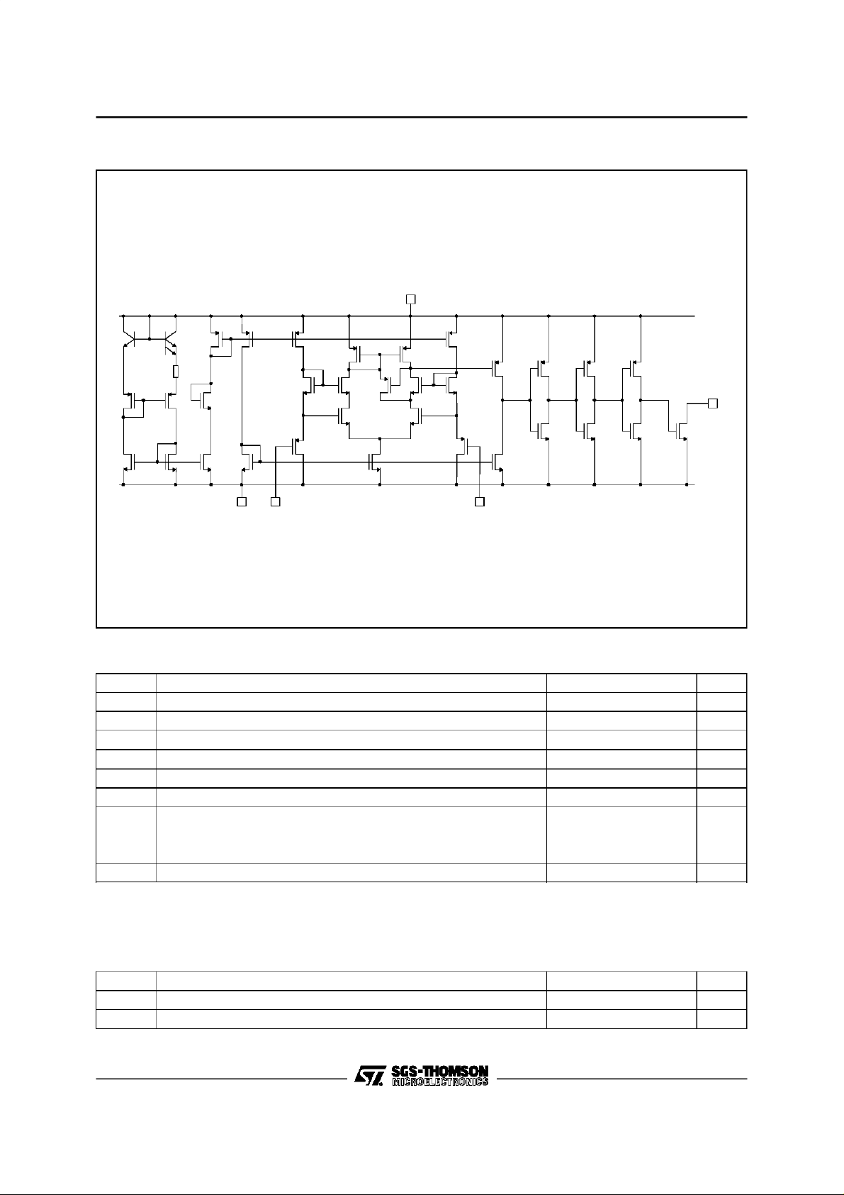
SCHEMATICDIAGRAM (for 1/4 TS374)
T
T
1
TT
34
T
5
T
T
2
7
R
1
T
T
6
T
9
10
8
T
12
T
13
T
T
11
-
V
Input - Input +
CC
14
T
16
T
15
T
18
T
17
T
19
+
V
CC
T
22
T
21
T
20
T
23
T
T
24
T
25
T
27
T
26
TT
30
31
T
32
Output
TT
33 34
T
28
29
MAXIMUMRATINGS
Symbol Parameter Value Unit
+
V
V
V
I
Supply Voltage - (note 1) 18 V
CC
Differential Input Voltage - (note2) ±18 V
id
Input Voltage- (note 3) 18 V
V
i
Output Voltage 18 V
O
Output Current 20 mA
O
Duration of Output Short-Circuit to GND - (note 4) Infinite
T
T
Notes : 1. All voltage values, except differential voltage,are with respect tonetwork ground terminal.
Operating Free-Air TemperatureRange
oper
Storage TemperatureRange -65 to +150
stg
2. Differential voltages are thenon-inverting input terminal with respect to the inverting input terminal.
3. The magnitude of theinput and the output voltages must never exceed the magnitude of thepositive supply voltage.
4. Short circuit fromoutputs to V
+
can cause excessiveheating and eventualdestruction.
CC
TS374C
TS374I
TS374M
0 to +70
-40 to +125
-55 to +125
OPERATINGCONDITIONS
Symbol Parameter Value Unit
+
V
V
2/5
Supply Voltage 3 to16 V
CC
Common Mode Input Voltage Range 0 to V
icm
CC
+
-1.5 V
o
C
o
C
TS374C,I,M
ELECTRICAL CHARACTERISTICSED
+
= 5V, V
V
CC
Symbol Parameter Min. Typ. Max. Unit
V
io
I
io
I
ib
V
icm
I
OH
V
OL
I
OL
I
CC
-
= 0V, T
CC
Input Offset Voltage(Vic=V
=25oC
T
amb
T
≤ T
min.
amb
=25oC (unlessotherwisespecified)
amb
) - (note 1)
icm min.
≤T
.
max
210
12
Input Offset Current- (note 2)
T
T
amb
min.
=25oC
≤ T
amb
≤T
. TS374C
max
TS374I/TS374M
1
100
200
Input Bias Current - (note 2)
=25oC
T
amb
T
≤ T
≤T
min.
amb
. TS374C
max
Input Common Mode Voltage Range
=25oC
T
amb
T
≤ T
≤T
min.
amb
. TS374C
max
TS374I/TS374M
TS374I/TS374M
0toV
0toV
0toV
CC
CC
CC
+
+
-2.25
+
-2
-2.5
1
150
300
High Level Output Current (Vid= 1V)
=25oCV
T
amb
T
≤ T
≤T
min.
amb
.V
max
Low Level Output Voltage(Vid= -1V,I
=25oC
T
amb
T
≤ T
≤T
min.
amb
max
.
OL=
4mA)
OH
OH
=5V
= 15V
0.1
1
100 400
700
Low Level Output Current (Vid= -1V,VOL= 1.5V) 6 45 mA
Supply Current (4 comparators) (Vid= +1V,no load) 0.6 1 mA
mV
pA
pA
V
nA
µA
mV
SWITCHINGCHARACTERISTICS (V
CC
+
= 5V, T
amb
=25oC)
Symbol Parameter Min. Typ. Max. Unit
t
Notes : 1. The specified offsetvoltage is themaximum value required todrive the outputdown to 400mV or up
Response Time (RL= 5.1kΩ connected to 5V,CL= 15pF - (note 3)
re
2. Maximum values including unavoidable inaccuracies of the industrial test.
3. The response time which isspecified is the internal between the inputsignal and the instant whenthe output signal crosses 1.4V.
• 100mV input step with 5mV overdrive
• TTL level input step
to 4V with R
=100kΩ to V
L
+
.
CC
600
200
ns
3/5
TS374C,I,M
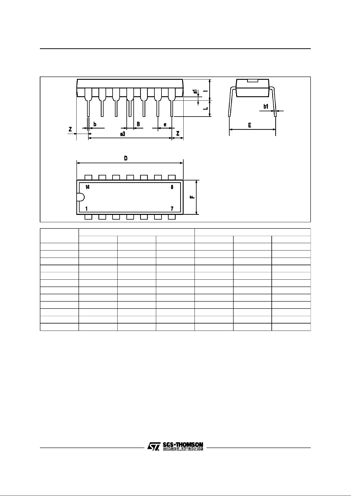
PACKAGE MECHANICAL DATA
14 PINS- PLASTICDIP
Dimensions
Min. Typ. Max. Min. Typ. Max.
Millimeters Inches
a1 0.51 0.020
B 1.39 1.65 0.055 0.065
b 0.5 0.020
b1 0.25 0.010
D 20 0.787
E 8.5 0.335
e 2.54 0.100
e3 15.24 0.600
F 7.1 0.280
i 5.1 0.201
L 3.3 0.130
Z 1.27 2.54 0.050 0.100
PM-DIP14.EPS
SO14.TBL
4/5
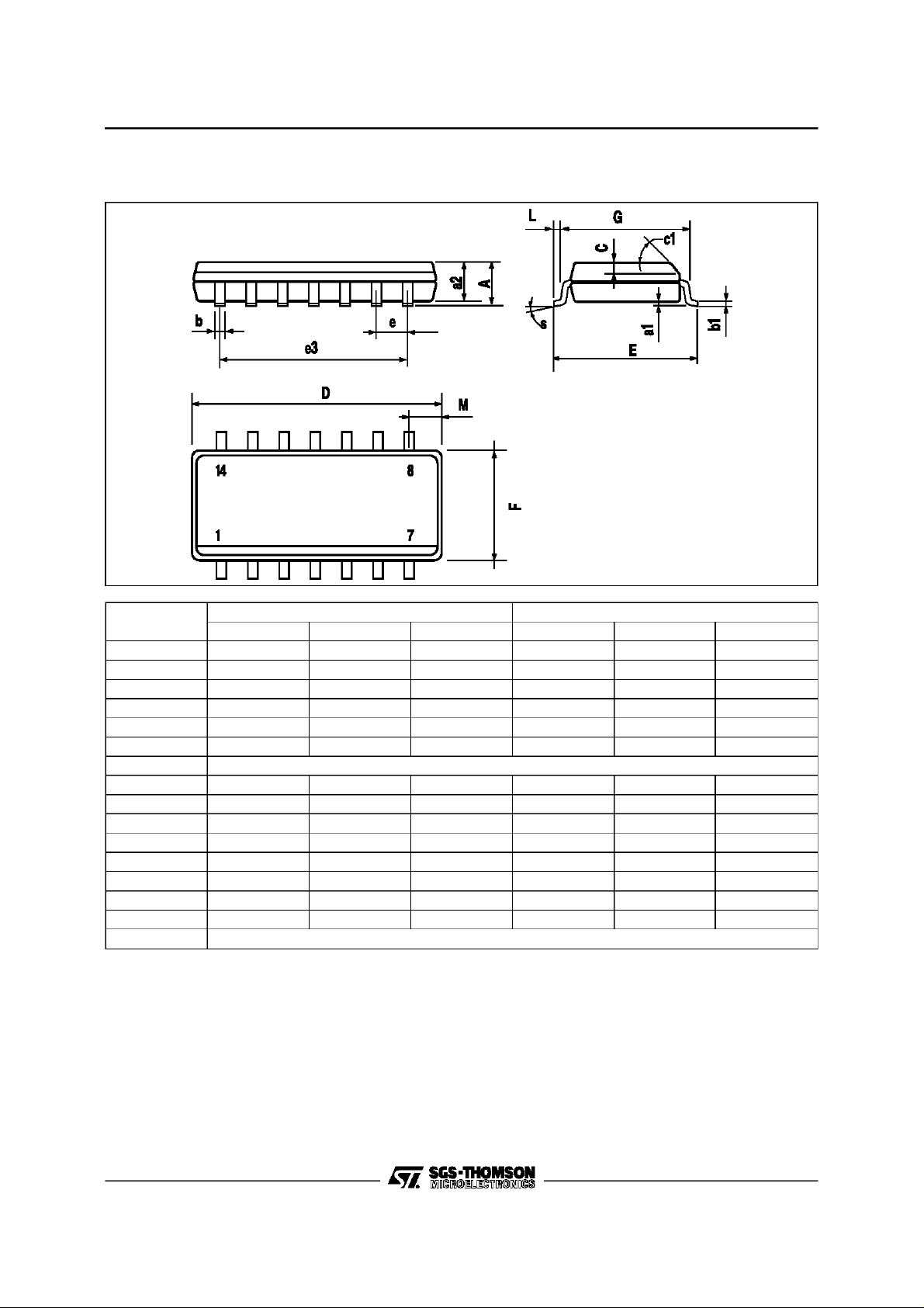
PACKAGE MECHANICAL DATA
14 PINS- PLASTICMICROPACKAGE(SO)
TS374C,I,M
Dimensions
Min. Typ. Max. Min. Typ. Max.
Millimeters Inches
A 1.75 0.069
a1 0.1 0.2 0.004 0.008
a2 1.6 0.063
b 0.35 0.46 0.014 0.018
b1 0.19 0.25 0.007 0.010
C 0.5 0.020
c1 45
o
(typ.)
D 8.55 8.75 0.336 0.334
E 5.8 6.2 0.228 0.244
e 1.27 0.050
e3 7.62 0.300
F 3.8 4.0 0.150 0.157
G 4.6 5.3 0.181 0.208
L 0.5 1.27 0.020 0.050
M 0.68 0.027
S8
Information furnished isbelieved to be accurate andreliable. However, SGS-THOMSON Microelectronics assumes no responsibility
for the consequences ofuse of suchinformation nor forany infringement ofpatents or other rightsof third parties which may result
from itsuse. No license is granted byimplication or otherwise under anypatent or patent rightsof SGS-THOMSON Microelectronics.
Specification mentioned in this publication are subject to change without notice. This publication supersedes and replaces all
information previously supplied.SGS-THOMSON Microelectronics productsare not authorized for useas critical componentsin life
support devices or systems withoutexpress written approval of SGS-THOMSON Microelectronics.
o
(max.)
PM-SO14.EPS
SO14.TBL
1997 SGS-THOMSON Microelectronics – Printed in Italy – AllRights Reserved
SGS-THOMSON Microelectronics GROUPOF COMPANIES
Australia - Brazil - Canada - China - France -Germany - Hong Kong - Italy -Japan - Korea - Malaysia - Malta- Morocco
The Netherlands - Singapore - Spain - Sweden - Switzerland -Taiwan - Thailand - United Kingdom - U.S.A.
ORDER CODE :
5/5

WWW.ALLDATASHEET.COM
Copyright © Each Manufacturing Company.
All Datasheets cannot be modified without permission.
This datasheet has been download from :
www.AllDataSheet.com
100% Free DataSheet Search Site.
Free Download.
No Register.
Fast Search System.
www.AllDataSheet.com
 Loading...