

SGS-THOMSON TEA2018A Technical data
POWER SUPPLY CONTROLCIRCUIT
.
DIRECT DRIVE OF THE EXTERNAL
SWITCHING TRANSISTOR
.
POSITIVE AND NEGATIVE OUTPUT CURRENTSUP TO 0.5 A
.
CURRENT LIMITATION
.
TRANSFORMER DEMAGNETIZATION
SENSING
.
FULL OVERLOAD AND SHORT-CIRCUIT
PROTECTION
.
PROPORTIONALBASECURRENT DRIVING
.
LOW STANDBY CURRENT BEFORE STARTING (< 1.6 mA)
.
THERMAL PROTECTION
DESCRIPTION
The TEA2018Aisan 8-pin DIP low-cost integrated
circuit designed for the control of switch mode
power supplies.
Due to its current mode regulation,the TEA2018A
facilitates design of power supplies with following
features :
.
High stability regulationloop
.
Automatic input voltage feed-forward in discontinuousmode fly-back
.
Automaticpulse-by-pulsecurrent limitation
Typical applications: VideoDisplayUnits, TVsets,
typewriters,microcomputersandindustrialapplications
Where synchronization is required, use the
TEA2019. For more details, see application
note AN406/0591
TEA2018A
CURRENT MODE SWITCHING
DIP8
(Plastic Package)
ORDER CODE : TEA2018A
PINCONNECTIONS
OSCILLATOR
COLLECTOR CURRENT SENSING
NEGATIVE SUPPLY VOLTAGE
May 1993
GROUND
1
2
3
4
8
ERROR AMPLIFIER NON-INVERTING INPUT
7
DEMAGNETIZATION SENSING
6
POSITIVE SUPPLY VOLTAGE
5
OUTPUT
2018A-01.EPS
1/7
TEA2018A
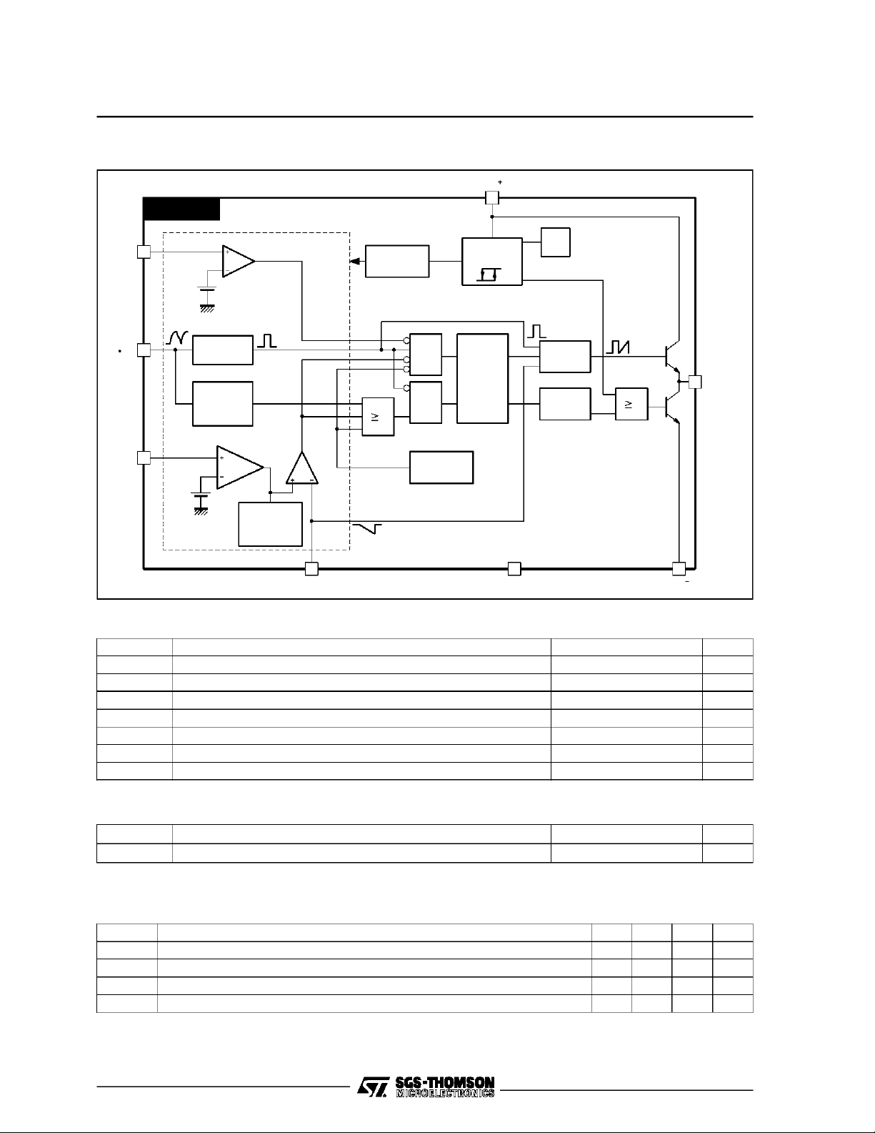
BLOCK DIAGRAM
TEA2018A
7
I
S
DEMAGNETIZATION
SENSING
INTERNAL
BIAS
V
CC
”Good”
V
CC
6
V
CC
MONITORING
V
REF
2.4V
Undervoltage0.1V
2.4V
OSCILLATOR1
MAXIMUM
DUTYCYCLE
70%
COMPARATOR
G ≅ 50
-1V
VOLTAGE
LIMITATION
I
SENSE
&
FLIP-FLOP
&
1
THERMAL
SHUTDOWN
3
GROUND
Ic
RECOPY
DELAY
500ns
5
OUTPUT
1
42
V
CC
RC
tt
8
ABSOLUTE MAXIMUM RATINGS
Symbol Parameter Value Unit
V
+ Positive Supply Voltage 15 V
CC
V
- Negative Supply Voltage -5 V
CC
I
(peak) Peak Output Current (duty cycle < 5%) ±1A
O
I
I
T
T
oper
T
stg
Input Current (Pin 3) ±5mA
Junction Temperature +150
j
Operating Ambient Temperature Range -20, +70
Storage Temperature Range -40, +150
o
C
o
C
o
C
2018A-02.EPS
2018A-01.TBL
THERMALDATA
Symbol Parameter Value Unit
R
th (j-a)
Junction-ambient Thermal Resistance 80
o
ELECTRICAL OPERATINGCHARACTERISTICS
=25oC, potentials referenced to ground (unless otherwise specified) (see testcircuit)
T
amb
Symbol Parameter Min. Typ. Max. Unit
V
+ Positive Supply Voltage 6.6 8 15 V
CC
V
- Negative Supply Voltage -1 -3 -5 V
CC
2/7
V
CC(start)
V
CC(stop)
Minimum Positive Supply Voltage required for starting (VCC+ rising) 6 6.6 V
Minimum Positive Voltage below wich device stopsoperating (VCC+ falling) 4.2 4.9 5.6 V
C/W
2018A-02.TBL
2018A-03.TBL

TEA2018A
ELECTRICAL OPERATINGCHARACTERISTICS
=25oC, potentials referenced to ground (unless otherwise specified) (see testcircuit)
T
amb
Symbol Parameter Min. Typ. Max. Unit
∆V
+ Hysteresis on VCC+ Threshold 0.7 1.1 1.6 V
CC
I
CC(sb)
V
th(IC)
R
V
τ
max
A
I
V
∆V
∆T
t
OSC
∆f
∆T
∆f
∆V
t
on(min)
Stand-by Supply Current before starting (VCC+<V
) 1 1.6 mA
CC(start)
Current Limitation Threshold Voltage (Pin 3) -1100 -1000 -880 mV
Collector Current Sensing Input Resistance 1000 Ω
(IC)
Demagnetization Sensing Threshold 75 100 125 mV
7(th)
I
Demagnetization Sensing Input Current (Pin7 = 0V) 1 µA
S
Maximum Duty Cycle 60 70 %
ErrorAmplifier Gain 50
V
+ Error Amplifier Input Current (non-inverting input) 2 µA
I
Internal Reference Voltage 2.3 2.4 2.5 V
REF
REF
ReferenceVoltage Temperature Drift 10
-4
Oscillator Free-running Period ( R = 59kΩ, C = 1.2nF) 44 48 52 µs
OSC
Oscillator Frequency Drift with Temperature (V
OSC
Oscillator Frequency Drift with VCC+ (+8V < VCC+ < +14V) 0.5 %/V
CC
+ = +8V) 0.05 %/oC
CC
Minimum Conducting Time (Ct= 1nF) 2 µs
V/oC
2018A-04.TBL
RECOMMENDEDOPERATINGCONDITIONS
Symbol Parameter Min. Typ. Max. Unit
V
+ Positive Supply Voltage 8 V
CC
V
- Negative Supply Voltage -3 V
CC
I
Output Current 0.5 A
O
f
oper
Operating Frequency 30 kHz
TEST CIRCUIT
V8 V7 V6
10
Ω
4321
470nF
22nF
59k
1%
1.2nF
1%
470
22nF
22nF
8765
Ω
TEA2018A
4.7nF
Ω
2018A-05.TBL
100Ω
V1 V3 V4
2018A-03.EPS
3/7
 Loading...