

查询TDA9105A供应商查询TDA9105A供应商
DEFLECTIONPROCESSOR FOR MULTISYNC MONITORS
TDA9105A
PRODUCT PREVIEW
HORIZONTAL
.
DUALPLLCONCEPT
.
150kHzMAXIMUM FREQUENCY
.
SELF-ADAPTATIVE
.
X-RAYPROTECTIONINPUT
.
DC ADJUSTABLEDUTY-CYCLE
.
1stPLLLOCK /UNLOCK INFORMATION
.
WIDE RANGE DC CONTROLLED H-POSITION
.
ON/OFF SWITCH (FOR PWR MANAGEMENT)
.
TWOH-DRIVE POLARITIES
VERTICAL
.
VERTICALRAMP GENERATOR
.
50 TO185Hz AGC LOOP
.
DCCONTR OLLE DV-A MP,V-PO S,S-AMP& C-COR
.
ON/OFFSWITCH
EWPCC
.
VERTICAL PARABOLA GENERATOR WITH
DCCONTROLLEDKEYSTONE& AMPLITUDE
.
AUTOTRACKINGWITH V-POS& V-AMP
.
CORNER CORRECTION WITH DC CONTROLLEDAMPLITUDE
GEOMETRY
.
WAVE FORM GENERATOR FOR PARALELLOGRAM& SIDE PIN BALANCECONTROL
.
AUTOTRACKINGWITH V-POS& V-AMP
DYNAMICFOCUS
.
VERTICALPARABOLAOUTPUTFOR VERTICALDYNAMICFOCUS
.
AUTOTRACKINGWITH V-POS& V-AMP
GENERAL
.
ACCEPT POSITIVE OR NEGATIVE HORIZONTAL& VERTICALSYNC POLARITIES
.
SEPARATEH & V TTL INPUT
.
COMPOSITEBLANKINGOUTPUT
DESCRIPTION
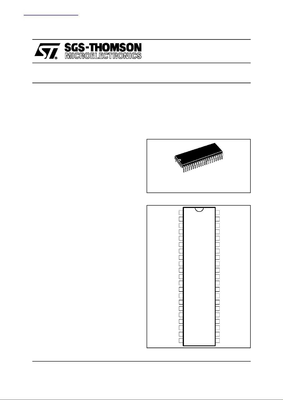
The TDA9105A is a monolithic integrated circuit
assembled in a 42 pins shrink dual in line plastic
package.
This IC controls all the functions related to the
horizontaland verticaldeflection in multimodesor
multisyncmonitors.
This IC, combined with TDA9205 (RGB preamp),
STV942x(OSDprocessor),ST727x(micro controller)and TDA817x(verticalbooster),allowsto realize very simple and high quality multimodes or
multisyncmonitors.
SHRINK42
(Plastic Package)
ORDER CODE : TDA9105A
PIN CONNECTIONS
V-FOCUS
H-LOCKOUT
PLL2C
H-DUTY
H-FLY
H-GND
H-REF
FC2
FC1
C0
R0
PLL1F
H-LOCKCAP
PLL1INHIB
H-POS
XRAY-IN
H-SYNC
V
GND
H-OUTEM
H-OUTCOL
1
2
3
4
5
6
7
8
9
10
11
12
13
14
15
16
17
18
CC
19
20
21
42
41
40
39
38
37
36
35
34
33
32
31
30
29
28
27
26
25
24
23
22
SPINBAL
KEYBAL
GEOMOUT
EWAMP
KEYST
EWOUT
V-FLY
VDCIN
V-SYNC
V-POS
VDCOUT
V-AMP
V-OUT
C-CORR
VS-AMP
V-CAP
V-REF
V-AGCCAP
V-GND
CORNER
BLK-OUT
9105A-01.EPS
July 1997
Thisis advanceinformation on a new product now in developmentor undergoingevaluation . Details are subject to changewithout notice.
1/31
TDA9105A
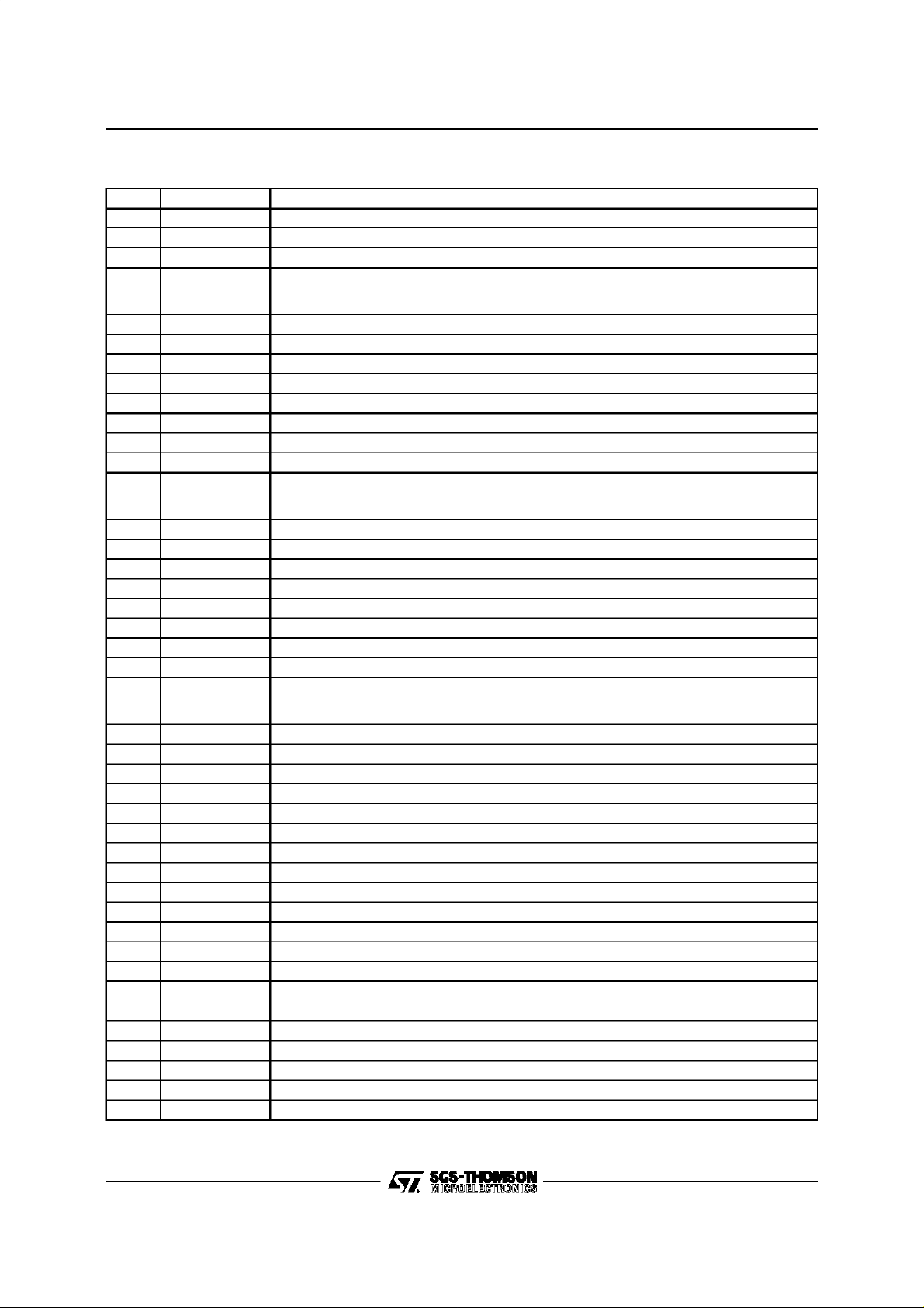
PIN DESCRIPTION
Pin Name Function
1 V-FOCUS Vertical Dynamic Focus Output
2 H-LOCKOUT First PLL Lock/Unlock Output
3 PLL2C Second PLL Loop Filter
4 H-DUTY DC Controlof HorizontalDriveOutput PulseDuty-cycle.If thisPin isgrounded, theHorizontal
5 H-FLY Horizontal Flyback Input (positive polarity)
6 H-GND Horizontal Section Ground
7 H-REF Horizontal Section Reference Voltage, must be filtered
8 FC2 VCO Low Threshold Filtering Capacitor
9 FC1 VCO High Threshold Filtering Capacitor
10 C0 Horizontal Oscillator Capacitor
11 R0 Horizontal Oscillator Resistor
12 PLL1F First PLL Loop Filter
13 H-LOCKCAP First PLL Lock/Unlock Time Constant Capacitor. When Frequency is changing, a Blanking
14 PLL1INHIB TTL-Compatible Input for PLL1 OutputCurrent Inhibition
15 H-POS DC Control for Horizontal Centering
16 XRAY-IN X-RAY protection Input (with internal latch function)
17 H-SYNC TTL compatible Horizontal Sync Input
18 V
CC
19 GND Ground
20 H-OUTEM Horizontal Drive Output (emiter of internal transistor)
21 H-OUTCOL Horizontal Drive Output (open collector of internal transistor)
22 BLK OUT BlankingOutput, activated during frequency changes, when X-RAY Input is triggered,when
23 CORNER DC Control of Corner Correction Amplitude
24 V-GND Vertical Section Signal Ground
25 V-AGCCAP Memory Capacitor for Automatic Gain Control Loop in Vertical Ramp Generator
26 V-REF Vertical Section Reference Voltage
27 V-CAP Vertical Sawtooth Generator Capacitor
28 VS-AMP DC Control of Vertical S-Shape Amplitude
29 C-CORR DC Control of Vertical C-Correction
30 V-OUT Vertical Ramp Output (with frequency independant amplitude and S-Correction)
31 V-AMP DC Control of Vertical Amplitude Adjustment
32 VDCOUT Vertical Position Reference Voltage Output
33 V-POS DC Control of Vertical Position Adjustment
34 V-SYNC TTL-Compatible Vertical Sync Input
35 VDCIN Geometric Correction Reference Voltage Input
36 V-FLY Vertical Flyback Input (positive polarity)
37 EWOUT East /West Pincushion Correction Parabola Output
38 KEYST DC Control of Keystone Correction
39 EWAMP DC Control East/West Pincushion Correction Amplitude
40 GEOMOUT Side Pin Balance & Parallelogram Correction Parabola Output
41 KEYBAL DC Control of Parallelogram Correction
42 SPINBAL DC Control of Side Pin Correction Amplitude
and VerticalOutputs are inhibited. By connectinga Capacitor on this Pin a Soft-startfunction
may be realized on H-drive Output.
Pulse is generated on Pin 23, the durationof this Pulse is proportionnal to the Capacitor on
Pin 13.
Supply Voltage (12V Typ.)
VS istoolow, or when Device is instand-bymode(through H-DUTYPin 2)andduringH-FLY,
V-FLY, V-SYNC, VSawth retrace.
9105A-01.TBL
2/31
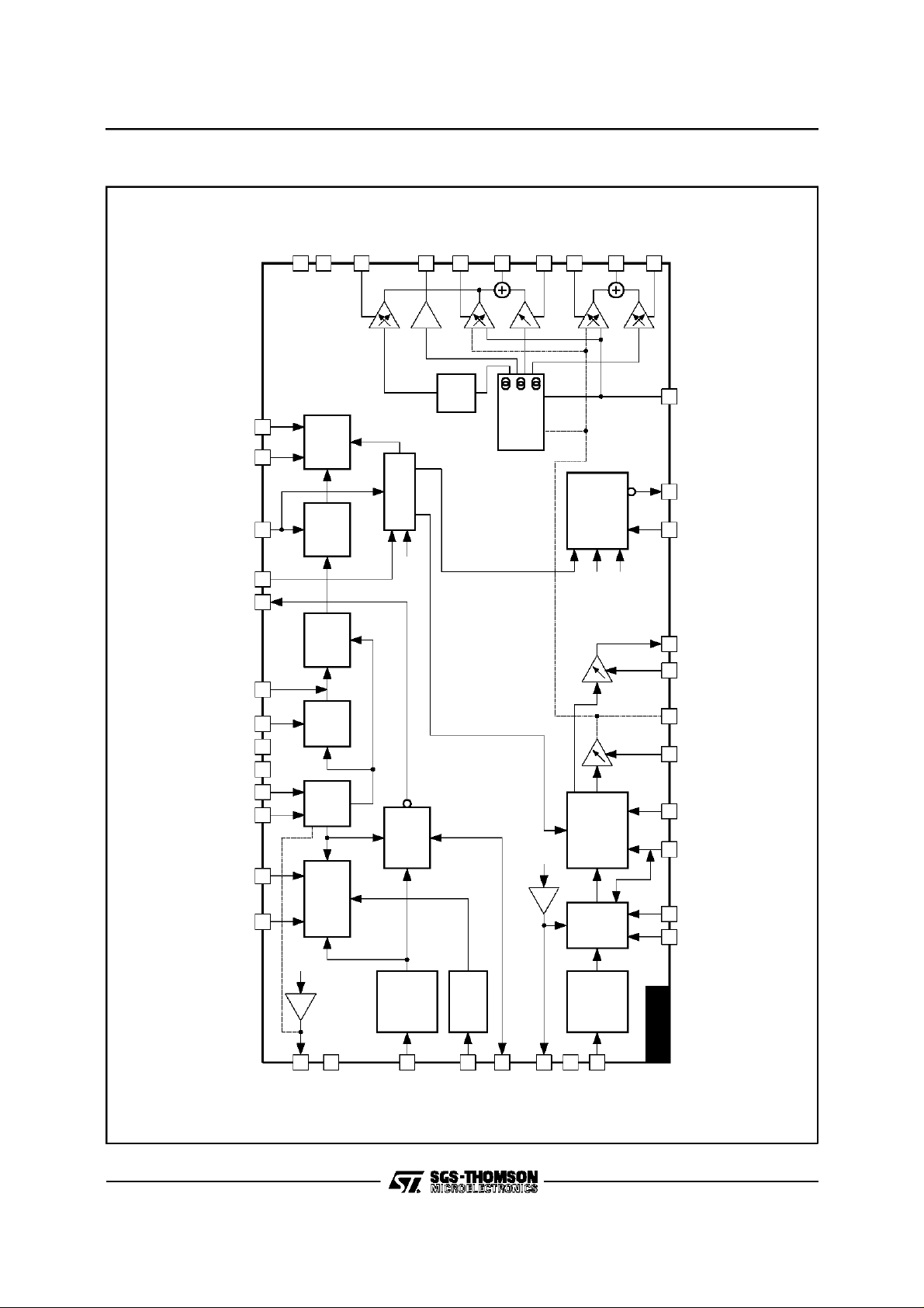
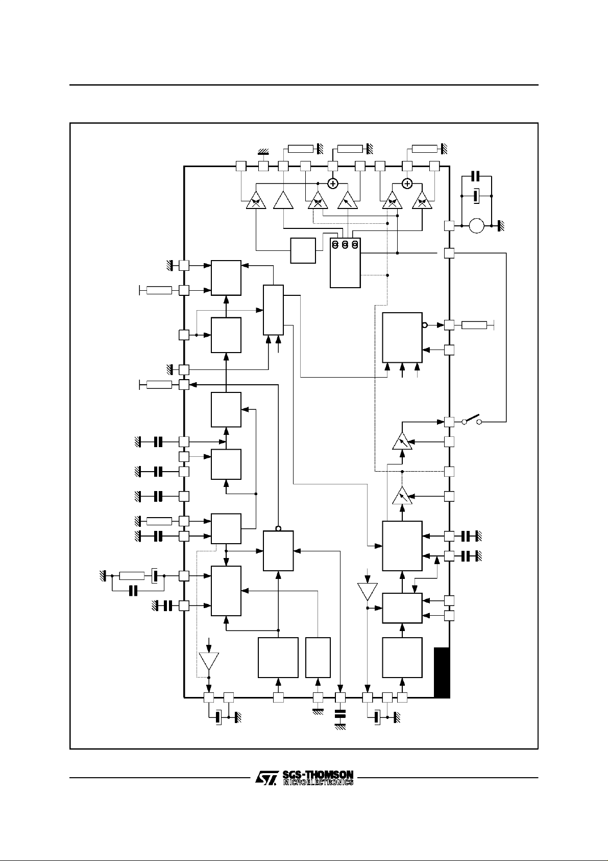
BLOCKDIAGRAM
GND18V
19
TDA9105A
CC
CORNER
23
V-FOCUS
1
38
KEYST
EWOUT
37
EWAMP
39
KEYBAL
41
GEOMOUT
SPINBAL
40
42
H-OUTEM
20
H-OUTCOL
21
H-DUTY
4
XRAY-IN
16
H-LOCKOUT
2
PLL2C
3
H-FLY
5
FC1
9
FC2
8
R0
11
C0
10
PLL1F
12
H
BUFFER
OUTPUT
PULSE
SHAPER
PHASE
SHIFTER
COMP
PHASE
VCO
SAFETY
PROCESSOR
VS
VIDEO UNLOCK
LOCK
IDENT
UNLOCK
2
X
2
X
BLK
GEN
H-FLY
V-SYNC
VDCIN
35
22
36
32
33
30
31
BLK-OUT
V-FLY
VDCOUT
V-POS
V-OUT
V-AMP
V-MID
VAGCCAP
VCAP
RAMP
VERT OSC
GENERATOR
25
27
V-REF
H-POS
COMP
15
PHASE
FREQUENCY
S
CORR
29
28
C-CORR
VS-AMP
V-REF
7
H-REF
6
H-GND
POL
PULSE
SHAPER
17
H-SYNC
DETECT
PLL1
INHIB
14
PLL1INHIB
13
26
V-REF
H-LOCKCAP
PULSE
24
V-GND
POL
DETECT
SHAPER
34
V-SYNC
TDA9105A
9105A-02.EPS
3/31
TDA9105A
QUICK REFERENCEDATA
Parameter Value Unit
Horizontal Frequency 15 to 150 kHz
Autosynch Frequency (for Given R0, C0) 1 to 3.7 FH
Hor Sync Polarity Input YES
±
Compatibility with Composite Sync on H-SYNC Input YES (see note 1)
Lock/Unlock Identification on 1
DC Control for H-Position YES
X-RAY Protection YES
Hor DUTY Adjust YES
Stand-by Function YES
Two Polarities H-Drive Outputs YES
Supply Voltage Monitoring YES
PLL1 Inhibition Input YES
Composite Blanking Output YES
Horizontal Moire Output NO
Vertical Frequency 35 to 200 Hz
Vertical Autosync (for 150nF) 50 to 185 Hz
Vertical S-Correction YES
Vertical C-Correction YES
Vertical Amplitude Adjustment YES
Vertical Position Adjustment YES
East/West Parabola Output YES
PCC (Pin Cushion Correction) Amplitude Adjustment YES
Keystone Adjustment YES
Corner Correction Adjustment YES
Dynamic Horizontal Phase Control Output YES
Side Pin Balance Amplitude Adjustment YES
Parallelogram Adjustment YES
Tracking of Geometric Corrections with V-AMP and V-POS YES
Reference Voltage YES (see note 2)
Mode Detection NO
Vertical Dynamic Focus YES
Notes : 1. Provided PLL inhibitioninput is used, seeapplication diagram on page 27.
2. One for Horizontal section and one for Verticalsection.
st
PLL YES
9105A-02.TBL
4/31
TDA9105A
ABSOLUTEMAXIMUM RATINGS
Symbol Parameter Value Unit
V
CC
V
IN
VESD ESD Succeptibility
T
stg
T
T
oper
THERMAL DATA
Symbol Parameter Value Unit
R
th (j-a)
HORIZONTAL SECTION
OperatingConditions
Symbol Parameter Test Conditions Min. Typ. Max. Unit
VCO
R0min Oscillator Resistor Min Value(Pin 11) 6 kΩ
C0min Oscillator Capacitor Min Value (Pin 10) 390 pF
Fmax Maximum Oscillator Frequency 150 kHz
HsVR Horizontal Sync Input Voltage(Pin 17) 0 5.5 V
INPUT SECTION
MinD MinimumInput Pulses Duration (Pin 17) 0.7 µS
Mduty Maximum Input Signal Duty Cycle(Pin 17) 25 %
OUTPUT SECTION
I5m Maximum Input Peak Current (Pin 5) 5 mA
HOI1
HOI2
DC CONTROL VOLTAGES
DCadj DC Voltage on DC Controls (Pins 4-15) V
Supply Voltage (Pin 18) 13.5 V
Max Voltage on Pins 4, 15, 28, 29, 31, 33, 38, 39, 41, 42
Pin 5
Pins 17, 34
Pin 16, 2, 22
Pin 14
Human Body Model, 100pF Discharge through 1.5kΩ
EIAJ Norm, 200pF Discharge through 0Ω
8
1.8
6
12
5
2
300
Storage Temperature -40, +150 °C
Max Operating Junction Temperature 150 °C
j
Operating Temperature 0, +70 °C
Junction-Ambient Thermal Resistance Max. 65 °C/W
Horizontal Drive Output Max Current
Pin 20
Pin 21
Sourced current
Sink current
=8V 2 6 V
REF-H
20
20
V
V
V
V
V
kV
V
9105A-03.TBL
9105A-04.TBL
mA
mA
9105A-05.TBL
5/31
TDA9105A
HORIZONTAL SECTION (continued)
(V
ElectricalCharacteristics
= 12V,T
CC
Symbol Parameter Test Conditions Min. Typ. Max. Unit
SUPPLY AND REFERENCE VOLTAGES
V
V
I
REF-H
V
I
REF-V
Supply Voltage (Pin 18) 10.8 12 13.2 V
CC
Supply Current (Pin 18) See Figure 1 45 65 mA
I
CC
Reference Voltage for Horizontal Section (Pin 7) I = 2mA 7.4 8 8.6 V
REF-H
Max Sourced Current on V
Reference Voltage for Vertical Section (Pin 26) I = 2mA 7.4 8 8.6 V
REF-V
Max Sourced Current on V
(Pin 7) 5 mA
REF-H
(Pin 26) 5 mA
REF-V
INPUT SECTION/PLL1
V
V
V
Horizontal Input Threshold Voltage (Pin 17) Low level voltage
INTH
VCO Control Voltage (Pin 12) V
VCO
VCO Gain, dF/dV (Pin12) R0 = 6.49kΩ, C0 = 680pF 17 kHz/V
COG
Hph Horizontal Phase Adjust (Pin 15) % of Horizontal period
f0 FreeRunning Frequency (adjustable by changing R0) R0 = 6.49kΩ, C0 = 680pF 25 27 29 kHz
CR PLL1 Capture Range
PLLinh PLL 1 Inhibition (Pin 14) PLL ON
(Typ. Threshold = 1.6V) PLL OFF
I
HLock0
V
HLock0
Max Output Current on HLock Output I
Low Level Voltage on HLock Output V2with I2= 10mA 0.25 0.5 V
SECOND PLL ANDHORIZONTALOUTPUT SECTION
FBth Flyback Input Threshold Voltage (Pin 5) See Figure 14 0.60 0.70 V
Hjit Horizontal Jitter See ApplicationDiagram
Horizontal Drive Output Duty-cycle
(Pin 20 or 21) (see Note)
HDmin
HDmax
Minimum
Maximum
HDvd Horizontal Drive Low Level Output Voltage Pin 20 to GND,
HDem Horizontal Drive High Level Output Voltage
(output on Pin 20)
XRAYth X-RAYProtectionInput Threshold Voltage(Pin16) TBD 8 TBD V
ISblkO Maximum Output Current on Composite Blanking
Output
VSblkO Low-Level Voltageon Composite Blanking Output
(Blanking ON)
Vphi2 Internal Clamping Voltage on 2nd PLL Loop Filter
Output (Pin 3)
V
Threshold Voltage to Stop H-out, V-out and to
OFF
activate BLKout (OFF mode when V
(Pin 4)
VSCinh Supply Voltage to Stop H-out , V-out when
< VSCinh (Pin18)
V
CC
Note : If H-drive is taken on Pin 20 (Pin 21 connected to supply), H-D is the ratio of low level durationto horizontal period.
If H-drive is taken on Pin 21 (Pin 20 grounded), H-D is the ratio of high level duration to horizontal period.
Inboth cases, H-D period driving horizontal scanning transistor off.
amb
Fh Min
Fh Max
=25°C)
4<VOFF
High level voltage 2
= 8V 1.6 to 6.2 V
REF-H
12.5 %
±
R0 = 6.49kΩ, C0 = 680pF
See conditions on Fig. 1
f0
3.7 x f0
V
14
V
14
2
2
80 ppm
(Pins 8-9)
=2V
V
4
=6V
V
4
V
4=VREF
- 500mV
31
54.5
33.2
57
61.5
1.1 1.7 V
V
21-V20,IOUT
Pin 21 to V
= 20mA
I
OUT
I
22
V
with I22= 10mA 0.25 0.5 V
22
Vmin
Vmax
V
4
)
= 20mA
,
CC
9.5 10 V
1.6
4.0
TBD 7.5 V
0.8 V
0.8 V
10 mA
35.5
59.5%%
10 mA
1V
kHz
kHz
V
%
V
V
9105A-06.TBL
6/31
TDA9105A
VERTICALSECTION
OperatingConditions
Symbol Parameter Min. Typ. Max. Unit
VSVR Vertical Sync Input Voltage (Pin 34) 0 5.5 V
VEWM Maximum EW Output Voltage (Pin 37) 6.5 V
VDHPCM Maximum Dynamic Horizontal Phase Control Output Voltage (Pin 40) 6.5 V
VDHPCm Minimum Dynamic Horizontal Phase Control OutputVoltage (Pin 40) 0.9 V
VDFm Minimum Vertical Dynamic Focus Output Voltage (Pin 1) 0.9 V
Rload Minimum Load for less than 1% Vertical Amplitude Drift (Pin 25) 65 M
Ω
9105A-07.TBL
Electrical Characteristics
(V
= 12V,T
CC
amb
=25°C)
Symbol Parameter Test Conditions Min. Typ. Max. Unit
I
BIASP
I
BIASN
VSth Vertical Sync Input Threshold Voltage (Pin 34) High-level
VSBI Vertical Sync Input Bias Current
V
V
V
BiasCurrent(currentsourcedbyPNPBase)(Pin28) For V28=2V 2 µA
Bias Current(Pins 29-31) (sinkedby NPN base) For V31= 6V, V29= 6V 0.5 µA
2
Low-level
= 0.8V 1 µA
V
(Current Sourced by PNP Base)
Voltage at Ramp Bottom Point (Pin 27) 2/8 V
RB
Voltageat RampTopPoint (with Sync) (Pin 27) 5/8 V
RT
Voltage at Ramp Top Point (without Sync)
RTF
(Pin 27)
34
VRT-0.1 V
0.8
V
V
REF-V
REF-V
VSW Minimum Vertical Sync Pulse Width (Pin 34) 5 µS
VSmDut Vertical Sync Input Maximum Duty-cycle
15 %
(Pin 34)
VSTD Vertical Sawtooth Discharge Time Duration
With 150nF cap 70
S
µ
(Pin 27)
VFRF Vertical Free RunningFrequency V
= 2V, V29grounded,
28
Measured on Pin 27
100 Hz
Cosc (Pin27) = 150nF
ASFR AUTO-SYNC Frequency (see Note 1) With C
RAFD Ramp AmplitudeDrift Versus Frequency V
50Hz < f < 185Hz
Rlin Ramp Linearity on Pin 30 V
Vpos Vertical Position Adjustment Voltage(Pin 32) V
V
V
I
VPOS
V
Max Current on Vertical Position Control Output
(Pin 32)
Vertical Output Voltage (Pin 30)
OR
(peak-to-peak voltage on Pin 30)
V31=2V
V
V
V
OUTDC
DC Voltage on Vertical Output (Pin30) See Note 2 7/16 V
V0I Vertical Output Maximum Current (Pin 30)
= 150nF 50 185 Hz
27
= 6V, C27= 150nF
31
grounded 0.5 %
28,V29
=2V
33
=4V
33
= 6V 3.65
33
100 ppm/Hz
3.2
3.5
3.8
±2mA
2
=4V
31
= 6V 3.75
31
3
4
5mA
±
3.3 V
V
V
2.2 V
V
V
REF-V
dVS Max Vertical S-Correction Amplitude
= 2V inhibits S-CORR
V
28
= 6V gives maximum S-CORR
V
28
Ccorr Max Vertical C-Correction Amplitude V
∆V/V
V/V
∆
V
V
at T/4
30pp
at 3T/4 TBD
30pp
=2V
29
=4V
29
= 6V TBD
29
-4
+4
-1.6
0
1.6
TBD %
%
TBD %
%
%
VFly Th Vertical Flyback Threshold (Pin 36) 1 TBD V
VFly Inh Inhibition of Vertical Flyback Input (Pin 36) See Note 1 V
I
BIAS DCIN
Notes : 1. It is thefrequency range for which the VERTICAL OSCILLATOR will automatically synchronize, using a single capacitor value on
Bias Current (Pin 35) (sourced by PNP base) For V35=V
Pin 27 and with a constant ramp amplitude.
2. Typically 3.5Vfor Vertical reference voltage typical value (8V).
32
- 0.5 V
REF
2
A
µ
9105A-08.TBL
7/31
TDA9105A
VERTICALSECTION(continued)
East/WestFunction
Symbol Parameter Test conditions Min. Typ. Max. Unit
EW
TDEW
EW
EW
Keytrack Keystone versus V-POS control
KeyAmp Keystone Amplitude Adjustment V
Notes : 1. When Pin36 > V
DC Output Voltage (see Figure 2) V33= 4V, V35=V32,
DC
DC Output Voltage Thermal Drift See Note 2 100 ppm/°C
DC
Parabola Amplitude V28= 2V, V29grounded,
para
Parabola Amplitude versus V-AMP
track
Control (tracking between V-AMP
and E/W)
(tracking between V-POS and EW)
A/B Ratio
B/A Ratio
-0.5V,Vflyinput isinhibited and verticalblankingon composite blankingoutput is replaced byvertical sawtooth
discharge time.
2. These parameters are not tested on each unit. They are measured during our internal qualification procedure which includes
characterization on batches comming from corners of our processes and also temperature characterization.
REF
= 4V, V23=4V
V
38
= 6V, V33= 4V,
V
31
V
35=V32,V38
V
39
V
39
= 2V, V29grounded
V
28
= 4V, V35=V
V
33
V38= 4V, V39= 6V, V23=4V
V
31
V
31
V
31
= 4V, V28= 2V, V29grounded,
V
23
= 6V, V38= 4V, V39=6V
V
31
= 2V, V35=V
V
33
V33= 6V, V35=V
= 4V, V31= 6V, V39=2V
23
V
38
V
38
V
38
= 4V, V23=4V
=6V
=2V
32
=2V
=4V
=6V
32
32
=4V
=2V
=6V
TBD 1.70
2.5 V
0
0.45
1.0
1.7
0.54
0.54
0
1.3
1.3
V
V
V
V
V
V
V
V
9105A-09.TBL
DynamicHorizontalPhase Control Function
Symbol Parameter TestConditions Min. Typ. Max. Unit
DHPC
TDDHPC
SPBpara SidePinBalance ParabolaAmplitude
SPBtrack Side Pinbalance Parabola Amplitude
ParAdj Parallelogram Adjustment Capability
Partrack Parallelogram versus V-posControl
DC Ouput Voltage (see Figure 3) V33= 4V, V35=V32,V41=4V 4 V
DC
DC Output Voltage ThermalDrift See Note 100 ppm/°C
DC
= 2V, V29grounded,
V
28
= 6V, V33= 4V,
(see Figure 3)
ve r sus V-amp C ontrol (tra c k ing
between V-amp and SPB )
A/B ratio (see Figure.3)
B/A ratio
(tracking between V-pos and DHPC)
A/B ratio
B/A ratio
V
31
V
35=V32,V41
V
42
V
42
= 2V, V29grounded,
V
28
= 4V, V35=V32,
V
33
= 4V, V42=6V
V
41
V
31
V
31
V
31
= 2V, V29grounded,
V
28
= 6V, V33= 4V,
V
31
V
35=V32,V42
V
41
V
41
= 2V, V29grounded,
V
28
= 6V, V41= 4V, V42=6V
V
31
= 2V, V35=V32,
V
33
= 6V, V35=V
V
33
=4V
=6V
=2V
=2V
=4V
=6V
=6V
=6V
=2V
32
TBD +1.45
- 1.45 TBD
0.36
0.82
1.45
TBD
TBD
0.12
0.12
0.53
0.53
V
V
V
V
V
9105A-10.TBL
8/31
TDA9105A
VERTICALSECTION(continued)
VerticalDynamic Focus Function
Symbol Parameter Test Conditions Min. Typ. Max. Unit
VDF
TDVDF
VDFAMP Parabola Amplitude versus V-amp
VDFKEY Parabola Assymetry versus V-pos
Corner
Amplitude
DC Output Voltage (see Figure 4) V33= 4V, V35=V
DC
DC Output Voltage ThermalDrift See Note 100 ppm/C
DC
= 2V, V29grounded,
V
28
= 4V, V35=V32,
(tracking between V-amp and VDF)
(see Figure 4)
Control (tracking between V-pos
and VDF)
A/B ratio
B/A ratio
Corner Amplitude Adjustment V
V
33
=2V
V
31
=4V
V
31
=6V
V
31
= 2V, V29grounded,
V
28
= 6V,
V
31
V
= 2V, V35=V32,
33
= 6V, V35=V
V
33
= 4V, V38= 4V, V39=2V
31
=2V
V
23
=4V
V
23
=6V
V
23
32
-0.84
-1.78
-3.14
0.42
32
0.42
Tracking Corner with V-amp V23=6V
=2V
V
31
=4V
V
31
=6V
V
31
Note : These parameters are not tested on each unit. They are measured during our internal qualification procedure which includes
characterization on batches comming from corners of our processes and also temperature characterization.
6V
-0.72
-1.57
-2.85
0.54
0.54
0.55
0.55
0.2
0.55
1.7
-0.6
-1.36
-2.56
V
V
V
0.64
0.64
V
PP
0
V
PP
V
PP
VPP
V
PP
V
PP
9105A-11.TBL
9/31
TDA9105A
Figure1 : TestingCircuit
1kΩ
CC
V
Ω
CORNER
23
10k
1
19
38
10kΩ
10kΩ
100nF
40
37
41
39
42
2.2µF
CC12V
18
V
2
X
2
X
35
H
BUFFER
21 20
OUTPUT
V
CC
1.8kΩ
10nF
SAFETY
416
PULSE
SHAPER
PROCESSOR
BLK
GEN
10kΩ
CC
V
36 22
VS
2
10kΩ
PHASE
22nF
47nF
47nF
53
SHIFTER
COMP
PHASE
6.49kΩ 0.1%
VIDEOUNLOCK
10 11 8 9
680pF 1%
4.7µF
15 12
1µF
VCO
COMP
PHASE
FREQUENCY
LOCK
IDENT
UNLOCK
V-MID
V-REF
H-FLY
V-SYNC
RAMP
VERT OSC
GENERATOR
S
CORR
470nF
1%
27 25 31 30 33 32
1%
150nF
28
10/31
7
V-REF
6
2.2µF
POL
PULSE
SHAPER
17
DETECT
PLL1
INHIB
14
13
220nF
262924
2.2µF
POL
PULSE
SHAPER
34
DETECT
TDA9105A
9105A-03.EPS
 Loading...