

现货库存、技术资料、百科信息、热点资讯,精彩尽在鼎好!
18W Hi-Fi AMPLIFIER AND 35W DRIVER
DESCRIPTION
The TDA2030Ais a monolithic IC in Pentawatt
package intended for use as low frequency class
AB amplifier.
With V
reliable applications without regulated supply and
for 35W driver circuitsusing low-cost complementary pairs.
The TDA2030A provides high output current and
hasvery low harmonic and cross-overdistortion.
Furtherthe deviceincorporatesa short circuitprotection system comprising an arrangement for
automaticallylimitingthe dissipatedpowersoas to
keep the working point of the output transistors
within their safe operating area. A conventional
thermalshut-downsystem is also included.
= 44V itis particularlysuited for more
S max
TDA2030A
PENTAWATT
ORDERING NUMBERS : TDA2030AH
TDA2030AV
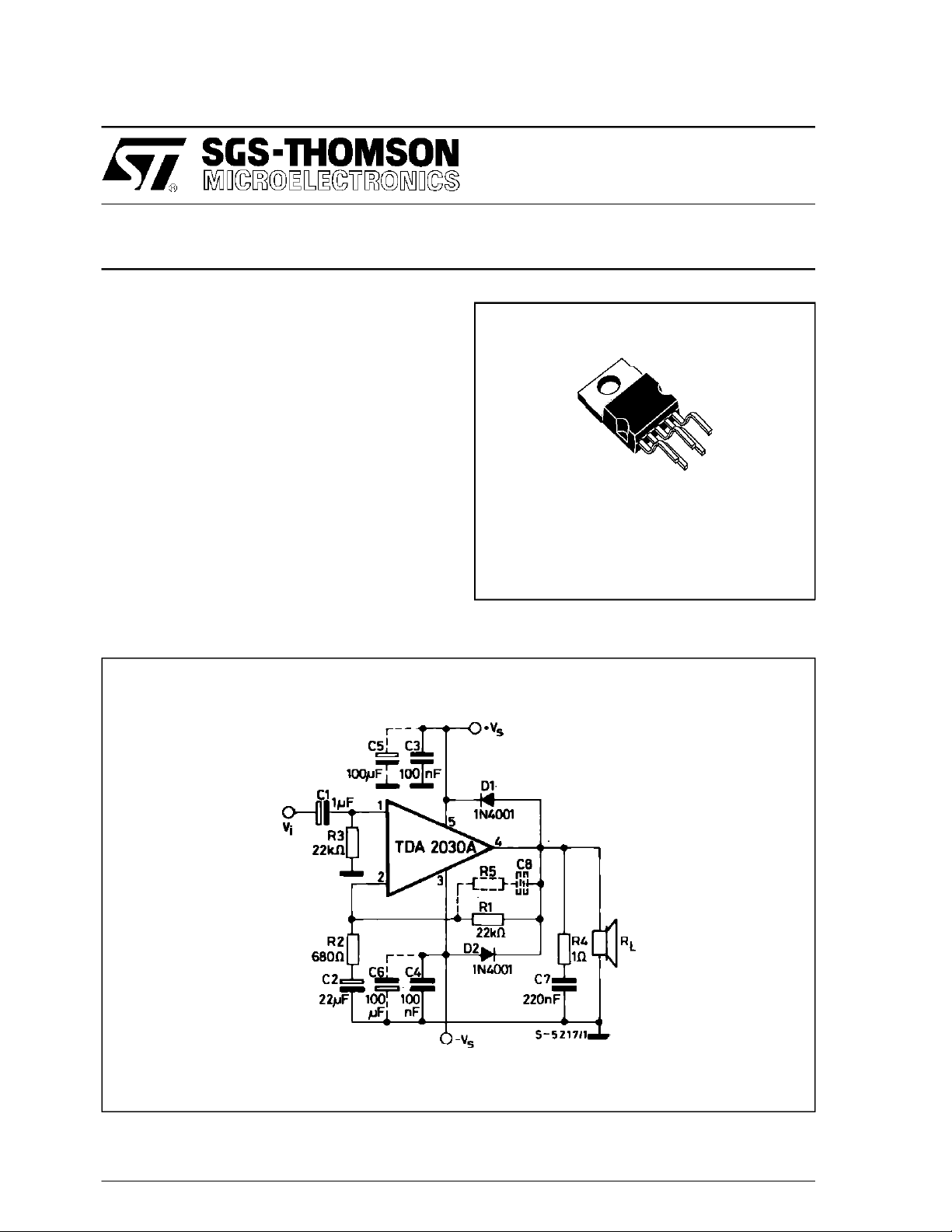
TYPICALAPPLICATION
March 1995
1/15
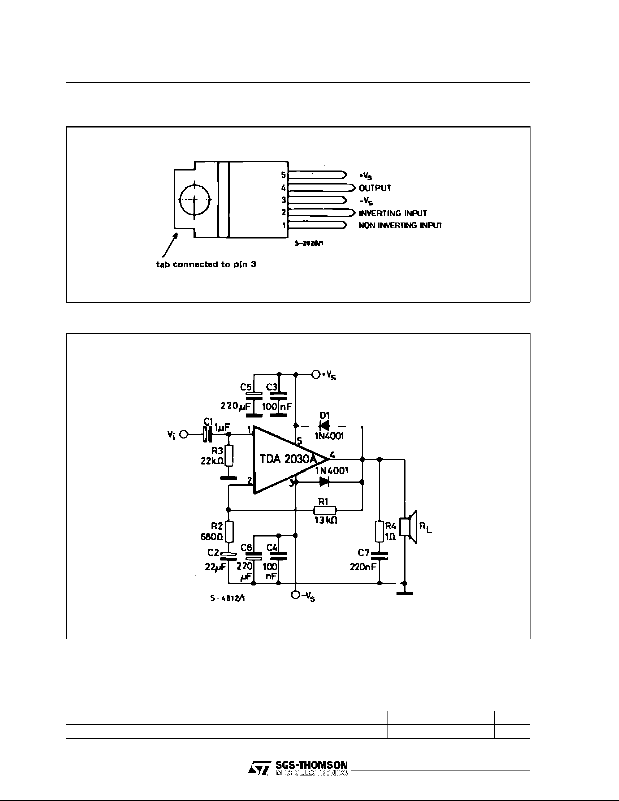
TDA2030A
PIN CONNECTION (Topview)
TESTCIRCUIT
THERMAL DATA
Symbol Parameter Value Unit
R
2/15
th (j-case)
Thermal Resistance Junction-case Max 3
°C/W

TDA2030A
ABSOLUTE MAXIMUMRATINGS
Symbol Parameter Value Unit
V
V
V
P
T
stg,Tj
ELECTRICALCHARACTERISTICS
(Refer to thetest circuit,V
Symbol Parameter Test Conditions Min. Typ. Max. Unit
V
V
I
P
BW Power Bandwidth
SR Slew Rate 8
G
G
d
d
e
S/N Signal to Noise Ratio
R
SVR Supply Voltage Rejection
T
Supply Voltage
s
Input Voltage V
i
Differential Input Voltage
i
I
Peak Output Current (internallylimited) 3.5 A
o
Total Power Dissipation at T
tot
case
=90°C
± 22
s
± 15
20 W
Storage and Junction Temperature – 40 to + 150 °
= ± 16V,T
S
Supply Voltage
s
I
Quiescent Drain Current 50 80 mA
d
Input Bias Current
I
b
Input Offset Voltage
os
Input Offset Current ±
os
Output Power d = 0.5%, Gv= 26dB
O
Open Loop Voltage Gain f = 1kHz 80 dB
v
Closed Loop Voltage Gain f = 1kHz 25.5 26 26.5 dB
v
d Total Harmonic Distortion
Second Order CCIF Intermodulation
2
Distortion
Third Order CCIF Intermodulation
3
Distortion
Input Noise Voltage B = Curve A
N
Input Noise Current B = Curve A
i
N
Input Resistance (pin 1) (open loop) f = 1kHz 0.5 5
i
Thermal Shut-down Junction
j
Temperature
=25oC unless otherwise specified)
amb
= ± 22V
V
S
= ± 22V ± 2 ± 20
V
S
f = 40 to 15000Hz
R
L
R
V
=±19V RL=8Ω
S
= 15W RL=4Ω 100 kHz
P
o
= 0.1 to 14W RL=4Ω
P
o
f = 40 to 15 000Hz f = 1kHz
= 0.1 to 9W, f = 40 to 15 000Hz
P
o
= 4W, f2–f1= 1kHz, RL=4Ω 0.03 %
P
O
L
R
L
f1= 14kHz, f2= 15kHz
= 13kHz
2f
1–f2
B = 22Hz to 22kHz
B = 22Hz to 22kHz
=4Ω,Rg= 10kΩ, B = Curve A
R
L
= 15W
P
O
=1W
P
O
=4Ω,Rg= 22kΩ
R
L
= 26dB, f = 100 Hz
G
v
=4Ω
=8Ω
=8Ω
± 6 ± 22
0.2 2
20 ± 200
15
18
10
12
13
16
0.08
0.03
0.5
0.08 %
2
310
50
80 200pApA
106
94
54 dB
145 °C
V/µsec
V
V
C
V
µA
mV
nA
W
%
%
%
µV
µV
dB
dB
MΩ
3/15
TDA2030A
Figure1 :SingleSupply Amplifier
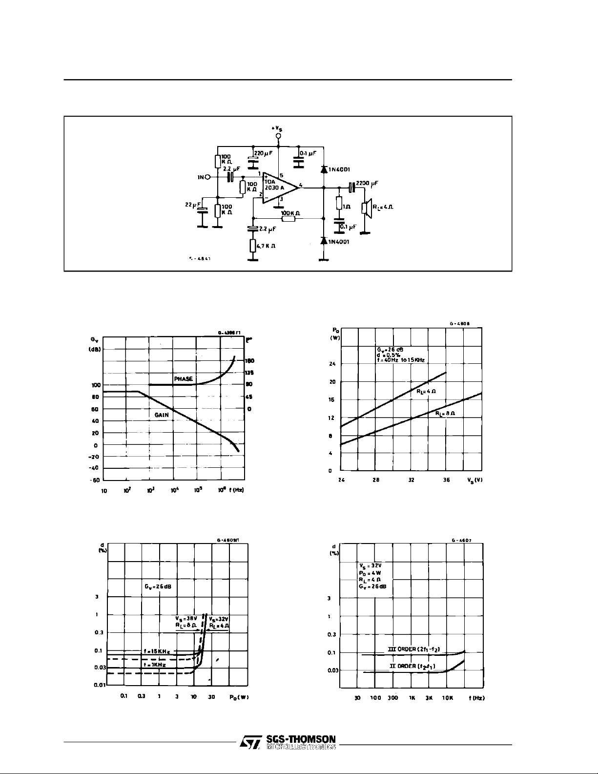
Figure2 : OpenLoop-frequencyResponse
Figure4 : TotalHarmonic Distortion versus
OutputPower (test using rise filters)
Figure 3 : Output Powerversus Supply Voltage
Figure 5 : Two ToneCCIF Intremodulation
Distortion
4/15
TDA2030A
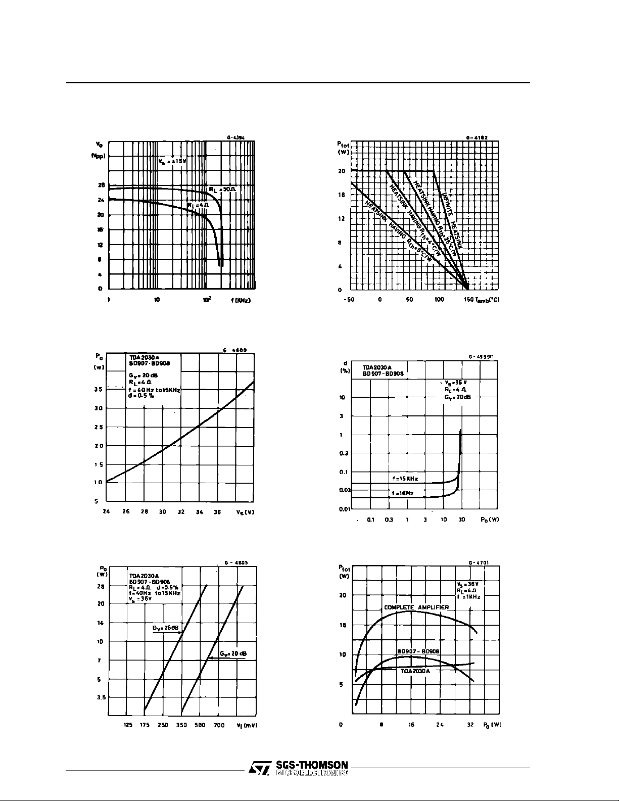
Figure6 : LargeSignal Frequency Response Figure 7 : MaximumAllowable Power Dissipation
versusAmbientTemperature
Figure8 : OutputPower versus Supply Voltage
Figure 9 : Total HarmonicDistortion versus
OutputPower
Figure10 : OutputPower versus Input Level Figure 11 : Power DissipationversusOutput
Power
5/15

TDA2030A
Figure12 : SingleSupply HighPower Amplifier (TDA2030A+ BD907/BD908)
Figure13 : P.C.Board and Component Layout for the Circuit of Figure 12 (1:1 scale)
6/15

TDA2030A
TYPICALPERFORMANCEOF THE CIRCUIT OF FIGURE 12
Symbol Parameter Test Conditions Min. Typ. Max. Unit
V
P
G
SR Slew Rate 8
V
S/N Signal to Noise Ratio
Figure14 : TypicalAmplifierwith SpiltPower Supply
Supply Voltage 36 44 V
s
Quiescent Drain Current Vs= 36V 50 mA
I
d
o
Output Power
d = 0.5%, R
d = 10%, R
Voltage Gain f = 1kHz 19.5 20 20.5 dB
v
d Total Harmonic Distortion f = 1kHz
= 20W f = 40Hz to 15kHz
P
o
Input Sensitivity
i
= 20dB, f = 1kHz, Po= 20W, RL=4Ω 890 mV
G
v
=4Ω,Rg= 10kΩ, B = Curve A
R
L
=4Ω, f = 40 z to 15Hz
L
=4Ω, f = 1kHz
L
V
s
V
s
V
s
V
s
P
o
P
o
= 39V
= 36V
= 39V
= 36V
= 25W
=4W
35
28
44
35
0.02
0.05
108
100
V/µsec
W
W
W
W
%
%
dB
Figure15 : P.C.Board and Component Layout for the Circuit of Figure 14 (1:1 scale)
7/15

TDA2030A
Figure16 : BridgeAmplifier with SplitPower Supply (PO= 34W, VS= ± 16V)
Figure17 : P.C.Boardand ComponentLayout for theCircuit of Figure16 (1:1 scale)
MULTIWAY SPEAKERSYSTEMSAND ACTIVE
BOXES
Multiway loudspeaker systems provide the best
possible acoustic performance since each loudspeaker is specially designed and optimized to
handle a limited range of frequencies.Commonly,
these loudspeaker systems divide theaudio spectrum intotwo or three bands.
To maintainaflat frequencyresponseovertheHi-Fi
audio range the bands covered by each loudspeakermust overlap slightly. Imbalance between
the loudspeakers produces unacceptable results
therefore it is important to ensure that each unit
generates the correct amount of acoustic energy
for its segmento of the audio spectrum. In this
respect it is also important to know the energy
distributionofthe music spectrumto determinethe
cutoff frequenciesof the crossoverfilters (seeFigure 18).As an example a 100Wthree-way system
with crossover frequencies of 400Hz and 3kHz
would require 50W for the woofer, 35W for the
midrange unit and 15W for thetweeter.
8/15

TDA2030A
Figure18 : Power Distribution versus Frequency
Both active and passive filters can be used for
crossoversbut today activefilters cost significantly
less than a good passive filter using air cored
inductors and non-electrolyticcapacitors. In addition, active filters do not suffer from the typical
defectsof passive filters:
- powerless
- increased impedance seen by the loudspeaker
(lowerdamping)
- difficulty of precise design due to variable loudspeaker impedance.
Obviously, activecrossovers can only be used if a
poweramplifieris provided for each drive unit.This
makes it particularlyinteresting and economically
soundto use monolithicpower amplifiers.
In someapplications, complex filters are not really
necessaryand simple RC low-passand high-pass
networks(6dB/octave)can be recommended.
The result obtained are excellent because this is
the best type of audio filter and the only one free
from phaseand transientdistortion.
The rather poor out of band attenuation of single
RC filters means that the loudspeaker must operate linearlywell beyondthe crossoverfrequencyto
avoid distortion.
A more effective solution, named ”Active Power
Filter” by SGS-THOMSONis shownin Figure 19.
Figure 19 : ActivePower Filter
The proposed circuit can realizecombined power
amplifiers and 12dB/octaveor 18dB/octavehighpass orlow-pass filters.
In practice, at the input pins of the amplifier two
equal and in-phase voltages are available, as required for the active filteroperation.
Theimpedanceat thepin(-) is of theorderof100Ω,
while that of thepin (+) isvery high, which is also
whatwas wanted.
The component values calculated for f
= 900Hz
c
using a Bessek3rd orderSallen and Keystructure
are :
C1=C2=C
22nF
3
R
1
8.2kΩ 5.6kΩ 33kΩ
R
2
R
3
Usingthistypeof crossoverfilter,a complete3-way
60W active loudspeaker system is shown in Figure 20.
It employs 2nd order Buttherworth filters with the
crossoverfrequenciesequal to 300Hz and 3kHz.
The midrangesection consistsof twofilters, a high
pass circuit followed by a low pass network. With
V
=36V theoutput power deliveredto thewoofer
S
is 25W at d = 0.06% (30Wat d = 0.5%).
The power delivered to the midrange and the
tweeter can be optimized in the design phase
taking in account the loudspeaker efficiency and
impedance(R
=4Ωto 8Ω).
L
It is quite common that midrange and tweeter
speakers have an efficiency 3dB higher thanwoofers.
9/15

TDA2030A
Figure20 : 3 Way60W ActiveLoudspeakerSystem(VS=36V)
10/15

TDA2030A
MUSICALINSTRUMENTS AMPLIFIERS
Another important field of application for active
systemsis music.
In this area the use of several medium power
amplifiers is more convenient than a single high
poweramplifier, and it isalso morerealiable.
A typical example (see Figure 21) consist of four
amplifiers each driving a low-cost, 12 inch loudspeaker. This application can supply 80 to
RMS
.
160W
Figure21 : HighPower Active Box
for Musical Instrument
TRANSIENT INTERMODULATION DISTORTION (TIM)
Transientintermodulation distortion is an unfortunate phenomen associated with negative-feedback amplifiers. When a feedback amplifier
receives an input signal which rises very steeply,
i.e.containshigh-frequencycomponents,the feedback can arrive too late so that the amplifiers
overloadsanda burst of intermodulationdistortion
will be produced as in Figure22. Sincetransients
occur frequently in musicthis obviouslya problem
for the designer of audio amplifiers.Unfortunately,
heavy negative feedbackis frequencyused to reduce the total harmonic distortion of an amplifier,
which tends to aggravate the transientintermodulation (TIM situation. The best known method for
the measurement of TIM consists of feeding sine
waves superimposed onto square waves, into the
amplifier under test. The outputspectrum is then
examined using a spectrum analyser and comparedto theinput.Thismethodsuffersfromserious
disadvantages: the accuracy islimited, the measurement is a ratherdelicate operation and an expensive spectrum analyser is essential. A new
approach (see Technical Note 143) applied by
SGS-THOMSONtomonolithicamplifiersmeasurementis fast cheap-itrequiresnothingmoresophisticatedthanan oscilloscope- and sensitive - and it
can be useddownto the valuesas low as 0.002%
in highpower amplifiers.
Figure 22 : OvershootPhenomenonin Feedback
Amplifiers
The ”inverting-sawtooh” method of measurement
isbasedon theresponseofanamplifier to a 20kHz
sawtoothwaveform.The amplifierhas no difficulty
followingthe slow ramp but itcannotfollowthefast
edge. The output will follow the upper line in Figure 23cutting ofthe shadedarea and thusincreasing themeanlevel. If this outputsignal isfilteredto
removethesawtooth,directvoltageremainswhich
indicates the amountof TIMdistortion, although it
is difficult to measure because it is indistinguishable fromthe DC offset of the amplifier. Thisproblem is neatly avoided in the IS-TIM method by
periodically inverting the sawtooth waveformat a
low audiofrequencyas shown in Figure24.
Figure 23 : 20kHz SawtoothWaveform
Figure 24 : Inverting SawtoothWaveform
11/15

TDA2030A
In the case of the sawtooth in Figure25 the mean
level was increased by the TIM distortion, for a
sawtoothin the otherdirectionthe oppositeis true.
The result is an AC signal at the output whole
peak-to-peakvalue is the TIM voltage, which can
be measured easily with an oscilloscope. If the
peak-to-peakvalue of the signal and the peak-topeak of the invertingsawtooth are measured, the
TIMcan be found verysimply from:
V
OUT
TIM=
V
sawtooth
⋅ 100
In Figure25 the experimentalresults are shownfor
the 30Wamplifierusing the TDA2030Aas adriver
and a low-cost complementarypair. A simple RC
filter on the input of the amplifier to limit the maximumsignalslope(SS)isaneffectivewaytoreduce
TIM.
Figure25 : TIMDistortion versus Output Power
Figure 26 : TIM DesignDiagram (f
= 30kHz)
C
POWERSUPPLY
Usingmonolithicaudioamplifierwithnon-regulated
supply voltage it is importantto designthe power
supply correctly. In any working case it must providea supply voltageless than themaximumvalue
fixed by the IC break-downvoltage.
It is essential to take into account all the working
conditions,inparticularmainsfluctuationsand supply voltage variations with and without load. The
TDA2030A(V
=44V) isparticularlysuitablefor
Smax
substitution of the standard IC power amplifiers
(with V
= 36V) for more reliable applications.
S max
An example, using a simple full-wave rectifier followed by a capacitor filter, is shown in the table 1
and in the diagramof Figure27.
The diagram of Figure 26 originated by SGSTHOMSONcanbeused to findthe Slew-Rate(SR)
requiredfor a givenoutput poweror voltageand a
TIMdesign target.
For example if an anti-TIM filter with a cutoff at
30kHz is used and the max. peak-to-peak output
voltage is 20V then, referring to the diagram, a
Slew-Rateof 6V/µs is necessaryfor 0.1%TIM.
As shown Slew-Rates of above 10V/µs do not
contributeto a furtherreductionin TIM.
Slew-Ratesof 100/µs arenotonlyuselessbutalso
a disadvantage in Hi-Fi audio amplifiers because
they tend to turnthe amplifierinto a radioreceiver.
12/15
Figure27 : DCCharacteristicsof
50W Non-regulated Supply

TDA2030A
Table 1
Mains
(220V)
+ 20% 28.8V 43.2V 42V 37.5V
+ 15% 27.6V 41.4V 40.3V 35.8V
+ 10% 26.4V 39.6V 38.5V 34.2V
– 10% 21.6V 32.4V 31.5V 27.8V
– 15% 20.4V 30.6V 29.8V 26V
– 20% 19.2V 28.8V 28V 24.3V
Secondary
Voltage
– 24V 36.2V 35V 31V
DC OutputVoltage (V
I
=0 Io= 0.1A Io=1A
o
)
o
Aregulatedsupplyisnot usuallyusedfor thepower
outputstagesbecauseof its dimensioningmust be
donetakingintoaccountthe power tosupplyinthe
signal peaks.They are only a smallpercentage of
the total music signal, with consequently large
overdimensioningof the circuit.
Evenifwitha regulatedsupplyhigheroutputpower
canbeobtained(V
isconstantin allworkingcondi-
S
tions), the additionalcostand power dissipationdo
notusuallyjustify its use. Usingnon-regulatedsupplies, there are fewer designe restriction. In fact,
when signal peaks are present, the capacitorfilter
actsasa flywheelsupplyingthe requiredenergy.
In average conditions, the continuouspower suppliedis lower. The music power/continuouspower
ratio is greater in this case than for the case of
regulated supplied, with space saving and cost
reduction.
APPLICATION SUGGESTION
The recommendedvalues of the componentsare
those shown on application circuit of Figure 14.
Differentvaluescan be used.The Table2 canhelp
the designer.
SHORT CIRCUIT PROTECTION
The TDA2030Ahas an original circuit which limits
the current of the output transistors. This function
can be considered as being peak power limiting
rather than simple current limiting. It reduces the
possibilitythat the device gets damaged duringan
accidentalshort circuitfrom AC output to ground.
THERMALSHUT-DOWN
The presenceof a thermallimiting circuitoffersthe
followingadvantages:
1. An overload on the output (even if it is
permanent), or an above limit ambient
temperaturecan beeasilysupported since the
T
cannotbe higher than150oC.
j
2. The heatsink can have a smaller factor of
safety compared with that of a conventional
circuit.Thereisnopossibility ofdevicedamage
due to high junction temperature. If for any
reason, the junctiontemperatureincreasesup
to 150
o
C, the thermal shut-down simply
reduces the power dissipation and the current
consumption.
Table 2
Comp.
R1
R2
R3
R4
R5
C1
C2
C3, C4
C5, C6
C7
C8
D1, D2 1N4001 To protect the device against output voltage spikes
(*) The value of closed loop gain must behigher than 24dB.
Recom.
Value
22kΩ Closed loop gain setting Increase of gain Decrease of gain
680Ω Closed loop gain setting Decrease of gain (*) Increase of gain
22kΩ Non inverting input biasing Increase of input impedance Decrease of input impedance
1Ω Frequency Stability Danger of oscillation at high
≅ 3R2
1µF
22µF
0.1µF
100µF
0.22µF
≈
2
πBR1
Upper Frequency Cut-off Poor High Frequencies
Input DC Decoupling Increase of low frequencies
Inverting DC Decoupling Increase of low frequencies
Supply Voltage Bypass Danger of Oscillation
Supply Voltage Bypass Danger of Oscillation
Frequency Stability Larger Bandwidth
1
Upper Frequency Cut-off Smaller Bandwidth Larger Bandwidth
Purpose
frequencies with inductive
loads
Attenuation
Larger than
Recommended Value
Smaller than
Recommended Value
Danger of Oscillation
cut-off
cut-off
13/15

TDA2030A
PENTAWATT PACKAGE MECHANICAL DATA
DIM.
MIN. TYP. MAX. MIN. TYP. MAX.
mm inch
A 4.8 0.189
C 1.37 0.054
D 2.4 2.8 0.094 0.110
D1 1.2 1.35 0.047 0.053
E 0.35 0.55 0.014 0.022
F 0.8 1.05 0.031 0.041
F1 1 1.4 0.039 0.055
G 3.4 0.126 0.134 0.142
G1 6.8 0.260 0.268 0.276
H2 10.4 0.409
H3 10.05 10.4 0.396 0.409
L 17.85 0.703
L1 15.75 0.620
L2 21.4 0.843
L3 22.5 0.886
L5 2.6 3 0.102 0.118
L6 15.1 15.8 0.594 0.622
L7 6 6.6 0.236 0.260
M 4.5 0.177
M1 4 0.157
Dia 3.65 3.85 0.144 0.152
A
H3
L
L1
C
D1
L5
Dia.
L7
L6
L2
L3
D
F1
H2
E
MM1
G1
G
F
14/15

TDA2030A
Information furnishedis believed to be accurate and reliable. However, SGS-THOMSON Microelectronics assumes no responsibility for the
consequences of use of such information nor for any infringementof patents or other rights of thirdparties which may result from its use. No
license is granted by implication or otherwise under any patentor patent rights of SGS-THOMSON Microelectronics. Specifications mentioned
in this publication are subject to change without notice. This publication supersedes and replaces all information previously supplied.
SGS-THOMSON Microelectronics products are notauthorized for useas critical components inlife supportdevices or systems withoutexpress
written approval of SGS-THOMSON Microelectronics.
1995 SGS-THOMSON Microelectronics - All Rights Reserved
PENTAWATTis a RegisteredTrademark of SGS-THOMSON Microelectronics
Australia - Brazil - France - Germany - Hong Kong - Italy - Japan- Korea -Malaysia- Malta - Morocco - TheNetherlands - Singapore -
SGS-THOMSON Microelectronics GROUP OF COMPANIES
Spain - Sweden- Switzerland - Taiwan - Thaliand -United Kingdom - U.S.A.
15/15
 Loading...