

现货库存、技术资料、百科信息、热点资讯,精彩尽在鼎好!
DESCRIPTION
The TDA1908 is a monolithic integrated circuit in
12 lead quad in-line plastic package intended for
lowfrequencypowerapplications.Themountingis
compatiblewith the old types TBA800, TBA810S,
TCA830Sand TCA940N. Its main featuresare:
– flexibility in use with a max output curent of 3A
and an operating supply voltage range of 4V to
30V;
– protectionagainst chip overtemperature;
– soft limiting in saturationconditions;
– low ”switch-on”noise;
– low numberof externalcomponents;
– high supplyvoltagerejection;
– very low noise.
TDA1908
8W AUDIOAMPLIFIER
Findip
ORDERING NUMBER : TDA1908
ABSOLUTE MAXIMUM RATINGS
Symbol Parameter Value Unit
V
s
I
o
I
o
P
tot
T
stg,Tj
Supply voltage 30 V
Output peak current(non repetitive) 3.5 A
Output peak current(repetitive) 3 A
Power dissipation: at T
Storage and junctiontemperature -40 to 150
=80°C
amb
at T
=90°C5W
amb
1W
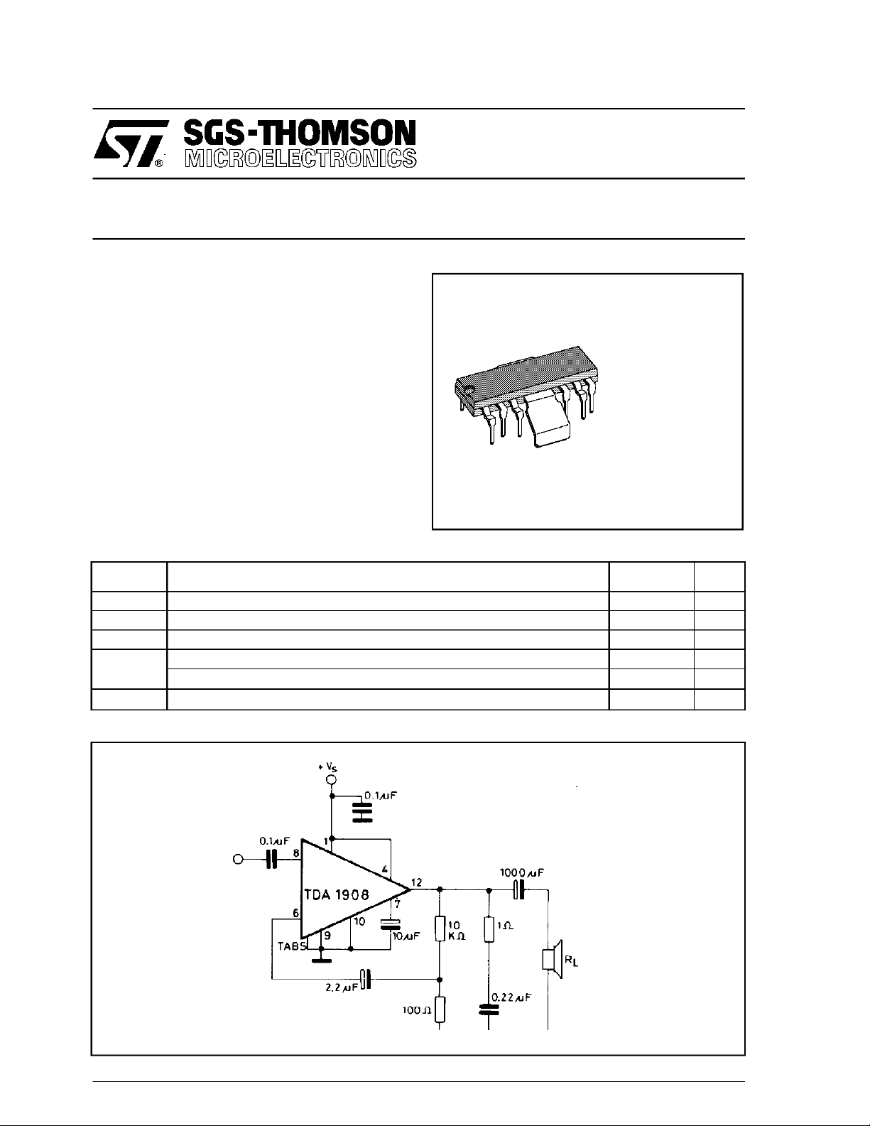
APPLICATION CIRCUIT
°C
March 1993
1/12
TDA1908
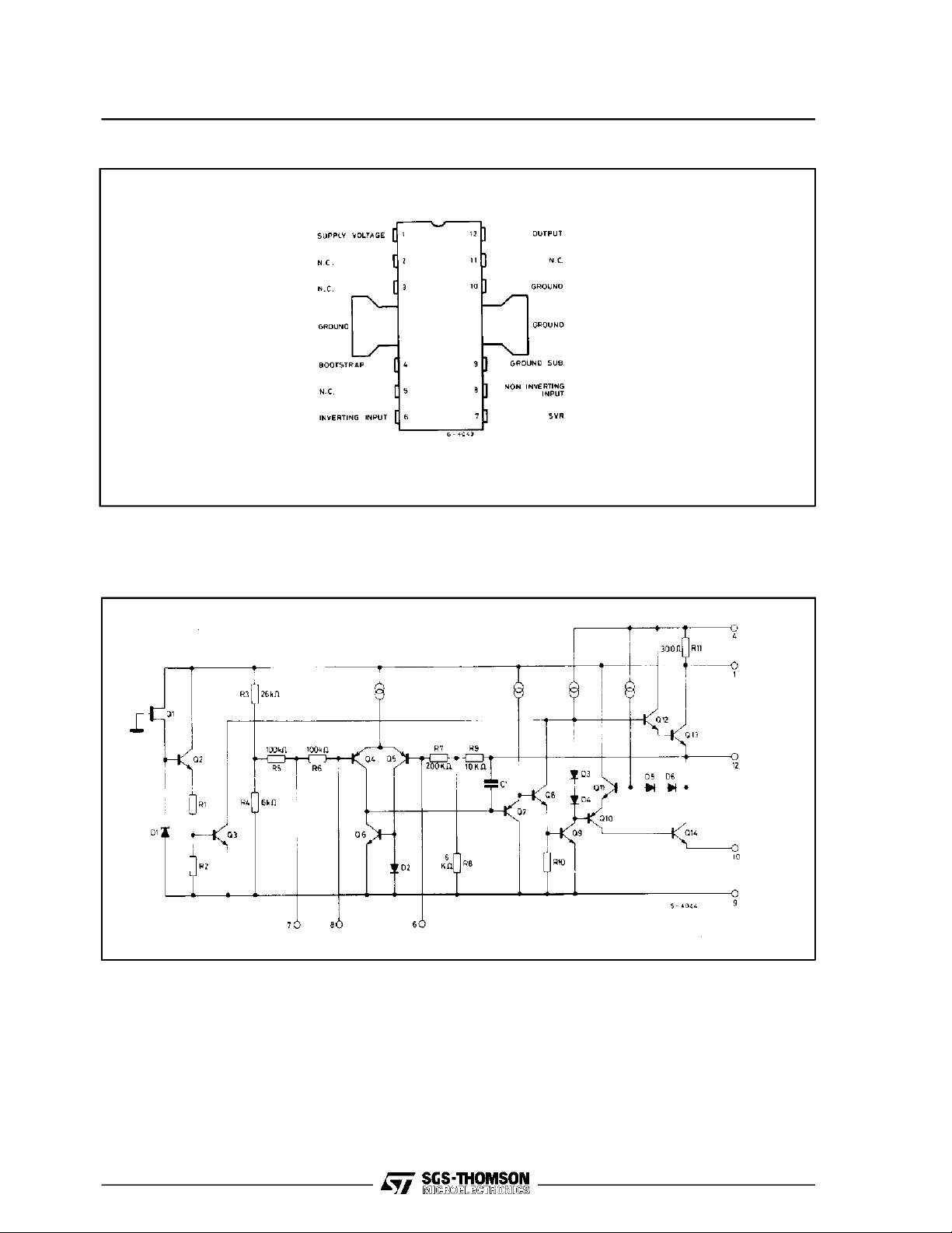
PIN CONNECTION(top view)
SCHEMATIC DIAGRAM
2/12
TDA1908
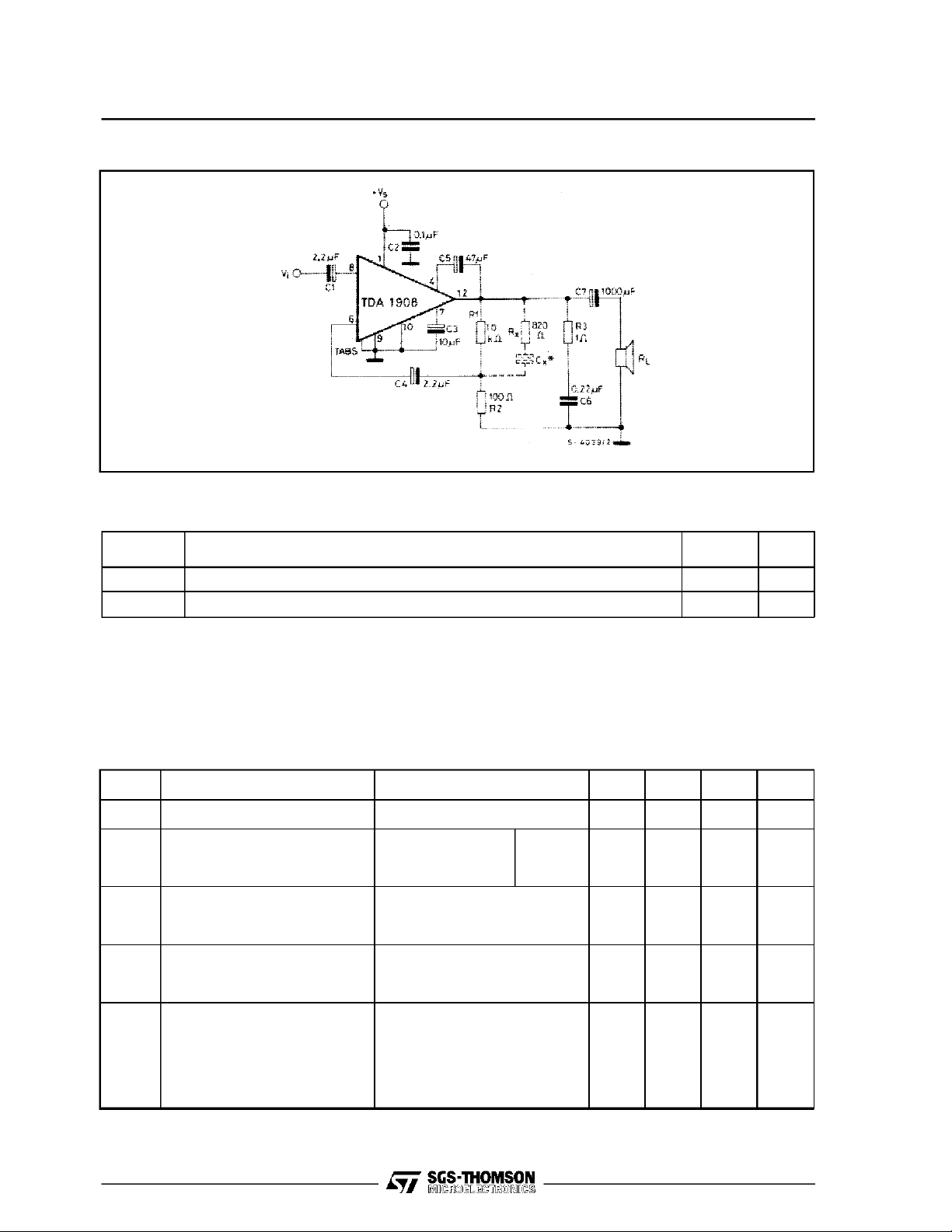
TEST CIRCUIT
* See fig. 12
THERMALDATA
Symbol Parameter Value Unit
R
th j-tab
R
th j-amb
(°) Obtained withtabs solteredto printed circuit board withmin copper area.
ELECTRICAL CHARACTERISTICS (Refertothetest circuit, T
Thermal resistancejunction-tab max 12
Thermal resistancejunction-ambient max (°)70
=25°C, Rth(heatsink)=8 °C/W, unless
amb
°C/W
°C/W
otherwisespecified)
Symbol Parameter Testconditions Min. Typ. Max. Unit
Supply voltage 4 30 V
V
s
2.5
10.2
16.8
V
Quiescent output voltage Vs=4V
V
o
I
Quiescent drain current Vs=4V
d
Output stage saturation voltage
CEsat
(each output transistor)
Output power
P
o
V
= 18V
s
V
= 30V
s
V
= 18V
s
V
= 30V
s
IC=1A
= 2.5A
I
C
d = 10% f = 1KHz
V
=9V RL=4Ω
s
V
= 14V RL=4Ω
s
V
= 18V RL=4Ω
s
V
= 22V RL=8Ω
s
V
= 24V RL=16Ω
s
1.6
8.2
14.4
7
6.5
4.5
2.1
9.2
15.5
15
17.5
21 35
0.5
1.3
2.5
5.5
9
8
5.3
V
mA
V
W
3/12

TDA1908
ELECTRICAL CHARACTERISTICS (continued)
Symbol Parameter Testconditions Min. Typ. Max. Unit
d Harmonic distorsion
Input sensivity Vs=9V
V
i
V
Input saturation voltage (rms) Vs=9V
i
R
Input resistence (pin 8) f = 1 KHz 60 100
i
I
Drain current f = 1 KHz
s
Efficiency
η
BW Small signal bandwitdth (-3 dB) V
f = 1KHz
V
=9V RL=4Ω
s
P
= 50 mW to 1.5 W
V
V
V
V
V
V
V
V
V
V
V
V
V
V
o
= 18V RL=4Ω
s
= 24V RL=16Ω
s
= 14V
s
= 18V
s
= 22V
s
= 24V
s
= 14V
s
= 18V
s
= 24V
s
= 14V
s
= 18V
s
= 22V
s
= 24V
s
= 18V f = 1 KHz
s
= 18V
s
=50mWto4W
P
o
P
=50mWto3W
o
=4Ω
R
L
R
=4Ω
L
R
=4Ω
L
R
=8Ω
L
R
=16Ω
L
R
=4Ω
L
R
=4Ω
L
R
=8Ω
L
R
=16Ω
L
R
=4Ω Po=9W
L
=4Ω
R
L
0.1
0.1
0.1
P
P
P
P
P
o
o
o
o
o
= 2.5W
= 5.5W
=9W
=8W
= 5.3W
37
52
64
90
110
0.8
1.3
1.8
2.4
P
P
P
P
o
o
o
o
= 5.5W
=9W
=8W
= 5.3W
570
730
500
310
72
P
= 1W 40 to 40 000 Hz
o
%
mV
V
KΩ
mA
%
G
Voltagegain (open loop) f = 1 KHz 75 dB
v
Voltagegain (closed loop)
G
v
Totalinput noise
e
N
S/N Signal to noise ratio
SVR Supply voltage rejection V
T
Termalshut-down junction
sd
temperature
Note :
(°) Weighting filter = curveA.
(° °) Filter with noisebandwidth: 22 Hz to22 KHz.
(*)
= 18V
V
s
f = 1 KHz
(°)
(°°)
= 18V
V
s
P
=9W
o
R
=4Ω
L
= 18V RL=4Ω
s
f
ripple
R
=4Ω
L
=1W
P
o
R
=50Ω
g
R
=1KΩ
g
R
= 10KΩ
g
=50Ω
R
g
R
=1KΩ
g
R
= 10KΩ
g
R
= 10KΩ
g
R
=0
g
R
= 10KΩ
g
R
=0
g
= 100 Hz Rg= 10KΩ
39.5 40 40.5 dB
1.2
1.3
1.5 4.0
2.0
2.0
2.2 6.0
(°)
(°°)
92
94
88
90
40 50 dB
145 ÉC
µV
µV
dB
dB
4/12
 Loading...