

现货库存、技术资料、百科信息、热点资讯,精彩尽在鼎好!
.
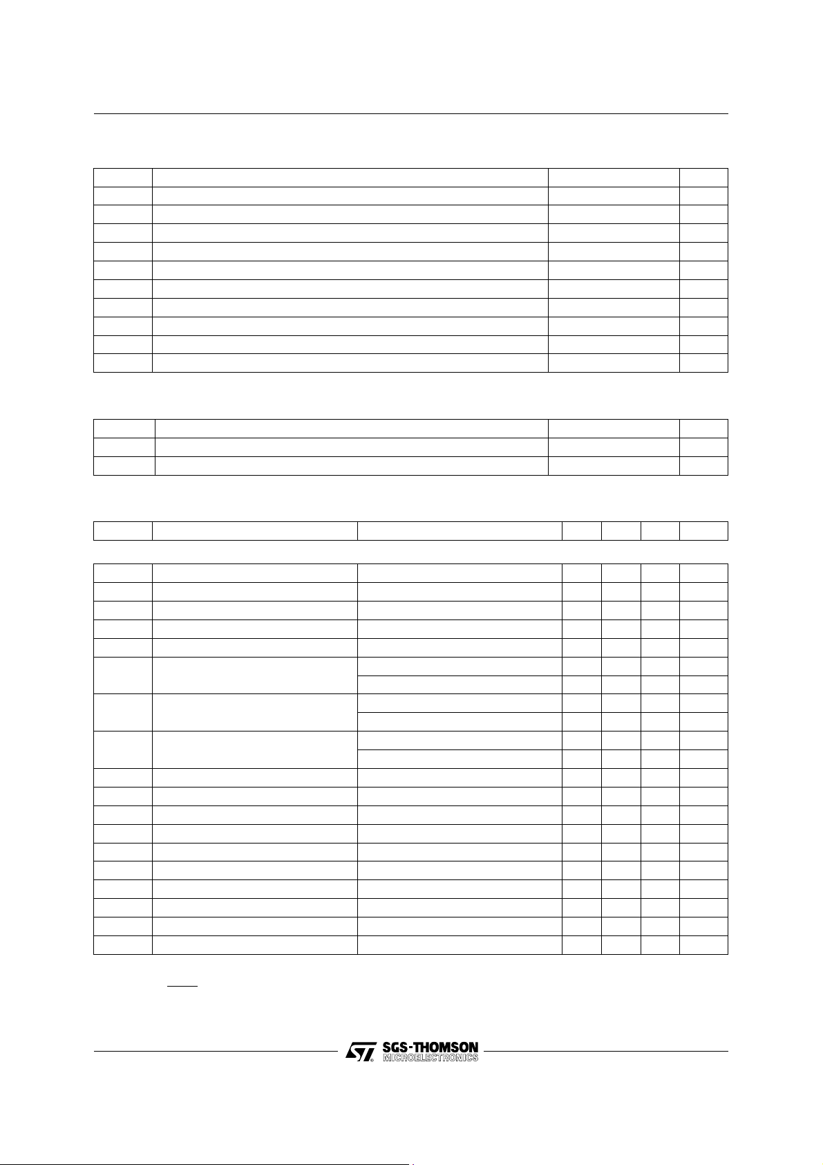
RAMP GENERATOR
.
INDEPENDENT AMPLI TUDE ADJUS TEMENT
.
BUFFER STAGE
.
POWER AMPLIFIER
.
FL YB AC K GENERATOR
.
INTERNAL REFERENC E VOLT A GE
.
THERMAL PROTECTIO N
TDA1771
VERTICAL DEFLECTION CIRC UIT
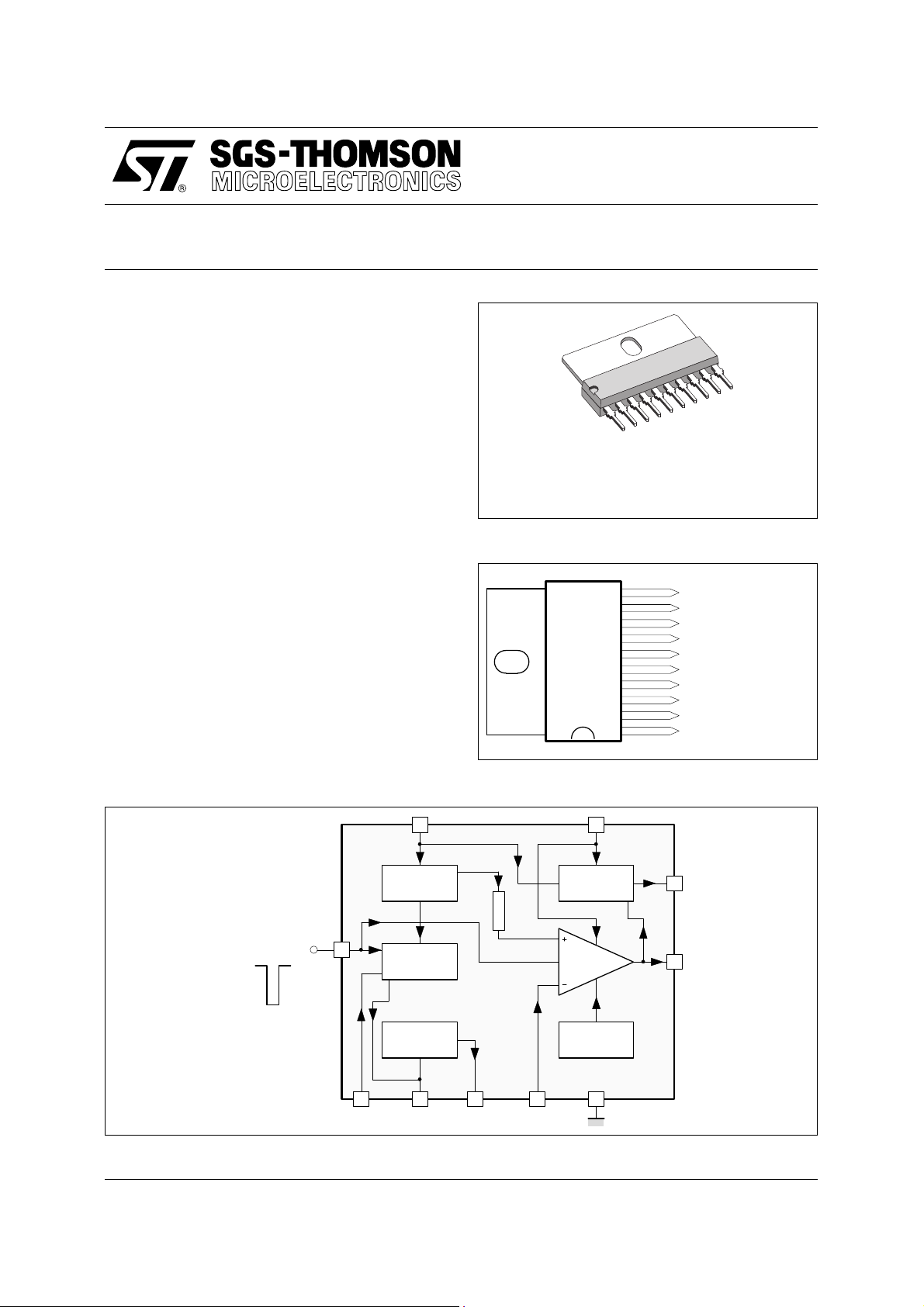
SIP10
(Plastic Package)
ORDER CODE : TDA1771
DESCRIPTION
The TDA1771 is a monolithic integrated circuit in
SIP10 package.
It is a full performance and very efficient vertical
deflection circuit intended for direct drive of a TV
picture tube in Color and B & W television as well
as in Monitor and Data displays.
BLOCK DIAGRAM
9
VOLTAGE
REGULATOR
TRIGGER IN
3
RAMP
GENERATOR
PIN CONNECTIONS (top view)
10
9
8
7
6
5
4
3
2
1
2
R3
CLOCK
PULSE
FLYBACK
GENERATOR
POWER
AMP.
10
1
FLYBACK GENERATOR
V
S
INVERTING INPUT
BUFFER OUTPUT
RAMP GENERATOR
GROUND
HEIGHT ADJUSTMENT
TRIGGER INPUT
OUTPUT STAGE V
POWER OUTPUT
S
1771-01.EPS
September 1993
BUFFER
STAGE
467 85
THERMAL
PROTECTION
1771-02.EPS
1/4
TDA1771
ABSOL UTE MAX IM UM R ATINGS
Symbol Parameter Value Unit
V
, V2Flyback Peak Voltage 65 V
V
1
V
V
I
I
P
T
S
THERMAL DATA
Symbol Parameter Value Unit
R
th (j-tab)
R
th (j-a)
Supply Voltage 30 V
S
Trigger Input Voltage 20 V
3
Amplifier Input Voltage GND to V
8
Output Peak to Peak Current (non repetitive t = 2ms) 6 A
I
0
Output Peak to Peak Current t > 10µs4A
I
0
Pin 10 DC Current at V1 < V
10
Pin 10 Peak to Peak Current @ t
10
Total Power Dissipation @ T
tot
9
< 1.5ms 3 A
fly
= 60°C9W
tab
S
100 mA
, TJStorage and Junction Temperature – 40, + 150 °C
Thermal Resistance Junction-tab Max. 10 °C/W
Thermal Resistance Junction-ambient Max. 70 °C/W
V
1771-01.TBL
1771-02.TBL
ELECTRICAL CHARACT E RIS TICS (T
= 25°C unless otherwise specified)
amb
Symbol Parameter Test Conditions Min. Typ. Max. Unit
DC (VS = 30V)
Pin 2 Quiescent Current I1 = 0, I10 = 0 16 36 mA
I
2
Pin 9 Quiescent Current I1 = 0, I10 = 0 15 30 mA
I
9
– I
– I
dI
V
V
V
V
dV
dV
V
Ramp Generator Bias Current V6 = 0 0.5 µA
6
Ramp Generator Current V6 = 0, – I4 = 20µA 18.5 20 21.5 µA
6
Ramp Gener. Linearity V6 = 0 to 15V, – I4 = 20µA0.21%
6/I6
Quiescent Output Voltage Ra = 30kΩ, Rb = 10kΩ, VS = 30V 17.0 17.8 18.6 V
1
= 6.8kΩ, Rb = 10kΩ, VS = 15V 7.2 7.5 7.8 V
R
a
Out Saturation Voltage to GND I1 = 0.5A 0.5 1 V
1L
= 1.2A 1 1.4 V
I
1
Out Saturation Voltage to V
1H
Reference Voltage – I4 = 20µA 6.3 6.6 6.9 V
4
Reference Voltage Drift Versus V
4/VS
Reference Voltage Drift Versus I
4/dI 4
Internal Ref. Voltage 4.26 4.40 4.54 V
r
S
– I1 = 0.5A 1.1 1.6 V
= 1.2A 1.6 2.2 V
– I
1
VS = 10V to 30V 1 2 mV/V
S
I4 = 10µA to 30µA 1.5 2 mV/µA
4
Gv Ouput Stage Open Loop Gain f = 100Hz 60 dB
V
V
fs
V
10
V
3
I
3
t
3
Notes : 1. The trigger input circuit can accept, with a metal option, positive and negative going input pulses.
2. th =
Saturation Voltage – I10 = 1.2A 1.5 2.5 V
9 – 10
Pin 10 Scanning Voltage I10 = 20mA 1.7 3 V
Trigger Input Threshold (see note 1) 2.6 3.0 3.4 V
Trigger Input Bias Current VIN = V3 – 0.2V 30 µA
Trigger Input Width (see note 2) 20 60 th µS
1.2 ⋅ t
S
where tS is the vertical period and VPP is ramp amplitude at Pin 6
V
PP
1171-03.TBL
2/4
 Loading...