

SGS-THOMSON TDA1180P Technical data

查询TDA1180供应商
■
NOISE GATED HORIZONTAL SYNC SEPARATOR
■
NOISE GATED VER T ICA L SY NC SE PARATOR
■
HORIZONTAL OSCILLATOR WITH FREQUENCY RANGE LIMITER
■
PHASE COMPARATOR BETWEEN SYNC
PULSES AND OSC ILLATOR P ULSE S (PLL)
■
PHASE COMPARATOR BETWEEN FLYBACK
PULSES AND OSC ILLATOR P ULSE S (PLL)
■
LOOP GAIN AND TIME CONSTANT SWITCHING ( VCR)
■
COMPOSITE BLANKING AND KEY PULSE
GENERATOR
■
PROTECTION CIRCUITS
■
OUTPU T S TAGES WI TH HI GH CURRENT CAPABILITY
TDA1180P
TV HORIZONTAL PROCESSOR
DIP16
(Plastic Package)
ORDER CODE : TDA1180P
DESCRIPTION
The TDA1 180P is a horizont al processor cir cuit for
b.w. and colour monitors. It is a monolithic integrated circuit encapsulated in 16-lead dual in-line
plastic package.
PIN CONNECTIONS
SUPPLY VOLTAGE
NEGATIVE OUTPUT
POSITIVE OUTPUT
PROTECTION CIRCUIT INPUT
PHASE SHIFTER FILTER
FLYBACK INPUT
KEY AND BLANKING PULSE OUTPUT
SYNC. SEPARATOR INPUT
1
2
3
4
5
6
7
8
16
15
14
13
12
11
10
GROUND
OSCILLATOR CONTROL CURRENT
OSCILLATOR
CONTROL CURRENT OUTPUT
TIME CONSTANT SWITCH
COINCIDENCE DETECTOR
VERTICAL SYNC. OUTPUT
9
VERTICAL SYNC. SEPARATOR INPUT
May 1993
1180P-01.EPS
1/12
TDA1180P
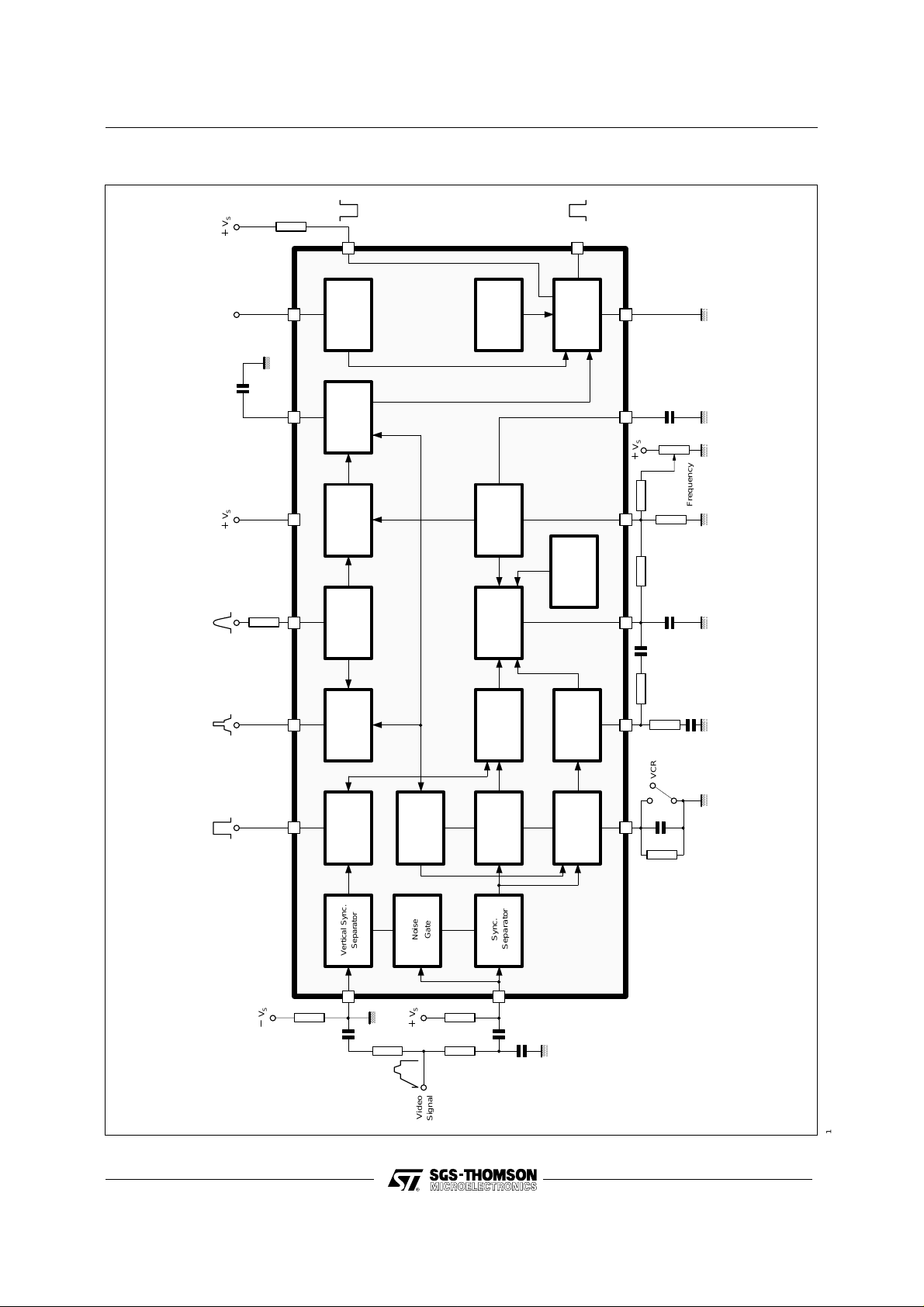
BLOCK DIAGRAM
S
V
2
Switch
Protection
and
Phase Shifter
Pulse Shaper
Under
Voltage
Protection
3
161415131211
Stage
Output
S
V
S
V
Phase
Flyback)
(Oscillator
Comparator
Pulse Shaper
and Blanking
Composite Key
Pulse Generator
1076154
Output Stage
Vertical Sync.
Separator
Vertical Sync.
Oscillator
Limiter
Voltage
Phase
Comparator
(Oscillator Sync .)
Blanking
Vertical Sync.
Gate
Pulse
Shaper
Gate
Noise
Sync.
Sync.
Separator
and Control
Time Constant
Current Switch
Detector
Coincidence
Frequency
VCR
2/12
S
V
9
S
V
Video
Signal
8
1180P-02.EPS
TDA1180P
ABSOL UTE MAX IM UM RAT INGS
Symbol Parameter Value Unit
V
V
V
V
V
V
I
P
T
stg
THERMAL DATA
Supply voltage (Pin 1) 15 V
S
Voltage at Pin 2 18 V
2
Voltage at Pin 4 V
4
Voltage at Pin 8 - 6 , V
8
Voltage at Pin 9 ± 6V
9
Voltage at Pin 11 V
11
I
Pin 2 peak current 1 A
2
Pin 3 peak current 0.5 A
I
3
I
Pin 6 current 30 mA
6
Pin 7 current 20 mA
I
7
Pin 10 current 30 mA
10
Total power dissipation at Tamb ≤ 70oC1W
tot
S
S
S
, TjStorage and junction temperature - 40 , + 150
V
o
C
1180P-01.TBL
Symbol Parameter Value Unit
R
th (j-a)
Thermal Resistance Junction-Ambient Max 80
ELECTRICAL CHARACTERISTICS
(refer to the test circuit, V
Symbol Parameter Test conditions Min. Typ. Max. Unit
V
V
HORIZONTAL SYNC. SEPARATOR
V
VERTICAL SYNC. SEPARATOR
V
V
R
t
t
Supply voltage range 9.5 12 13.2 V
S
Supply current I3 = 0 42 52 mA
I
S
Supply voltage at which the output pulses
S
(at pin 2 and 3) are switched off
Peak to peak input signal 1 3 6 V
V
I
Input switching voltage I8 = 80 µA 1.5 V
8
Input switching current V8 = 1.4V 10 µA
I
8
Leakage current V8 = -5V 1 µA
I
8
Peak to Peak Input Signal 1 3 6 V
V
I
Input Switching Voltage I9= 80µA 1.5 V
9
Input Switching Current V9 = 1.4V 5 µA
I
9
Leakage Current V9 = -5V 1 µA
I
9
Vertical Sync. Pulse Output Voltage No Load Pin10 11 V
10
Output Resistance 10 kΩ
10
Delay between Leading Edge of Input and Output
LV
Signals
Delay between Trailing Edge of Input and Output
LV
Signals
t
Vertical Sync Pulse Duration 190 µs
V
= 12V, TA = 25oC, unless otherwise specified)
S
4V
17 µs
50 µs
o
C/W
1180P-02.TBL
1180P-03.TBL
3/12
TDA1180P
ELECTRICAL CHARACT E RISTICS (continued)
(refer to the test circuit, V
Symbol Parameter Test conditions Min. Typ. Max. Unit
PROTECTION CIRCUIT
V
R
FLYBACK PULSE
V
V
OUTPUT PULSE
V
R
COMPOSITE BLANKING AND KEY PULSE
V
V
R
t
t
INTERNAL GATING PULSE
COINCIDENCE DETECTOR
V
I
VCR SWITCH
V
- I
I
TIME CONSTANT SWITCH
V
R
Input Voltage for Switching off the Output Pulses Output Pulses OFF
4
Input Resistance 200 kΩ
4
Input Current 5 µA
I
4
Input Threshold Voltage of Blanking Generator 1.8 V
6
Input Threshold Voltage of Phase Comparator 7.6 V
6
Input Switching Current V6 ≥ 1.7V 0.45 mA
I
6
Peak-to-Peak Output Voltage I3 = 150 mApp 10 V
3
Output Current V3 = 5V 500 mA
I
3
Output Resistance At Leading Edge of
3
Output Pulse Duration 20 22 26 µs
t
p
Key Pulse Output Peak Voltage 9 11 V
7k
Blanking Pulse Output Voltage 4.2 4.5 4.8 V
7B
Output Resistance 100 Ω
7
Phase Relation Between Trailing Edge of Key
sk
Pulse and Middle of Sync. Input Pulse
Key Pulse Duration 3.5 3.8 µs
t
k
Delay between Flyback Pulse and Blanking Pulse V6 = 1.7V 0.2 µs
fb
Gating Pulse Duration 7.5 µs
t
g
t Phase Relation between Middle of Sync. Pulse
and Trailing and Leading Edge of Gating Pulse
Output Voltage With Coincidence
11
Peak Output Current 0.5 mA
11
Input Voltage 0 to 4 or 8.5 to 12 V
11
Output Current 35 µA
11
Output Current 0.4 mA
11
Output Voltage 3V
12
Output Resistance 4.5V < V11 < 8V
12
= 12V, TA = 25oC, unless otherwise specified)
S
Output Pulses ON 1
output pulse
At Training Edge of
Output Pulse
Without Coincidence
> 8.5V or V11 < 4V
V
11
0.5 V
3
20
2.7 µs
3.75 µs
6.8
4
100
40
Ω
Ω
V
V
Ω
kΩ
1180P-04.TBL
4/12
 Loading...