

查询TDA1175供应商
LOW-NOISE VERTICALDEFLECTIONSYSTEM
.
COMPLETEVERTICAL DEFLECTION
SYSTEM
.
LOW NOISE
.
SUITABLEFOR HIGH DEFINITION
MONITORS
.
ESD PROTECTED
TDA1175P
DESCRIPTION
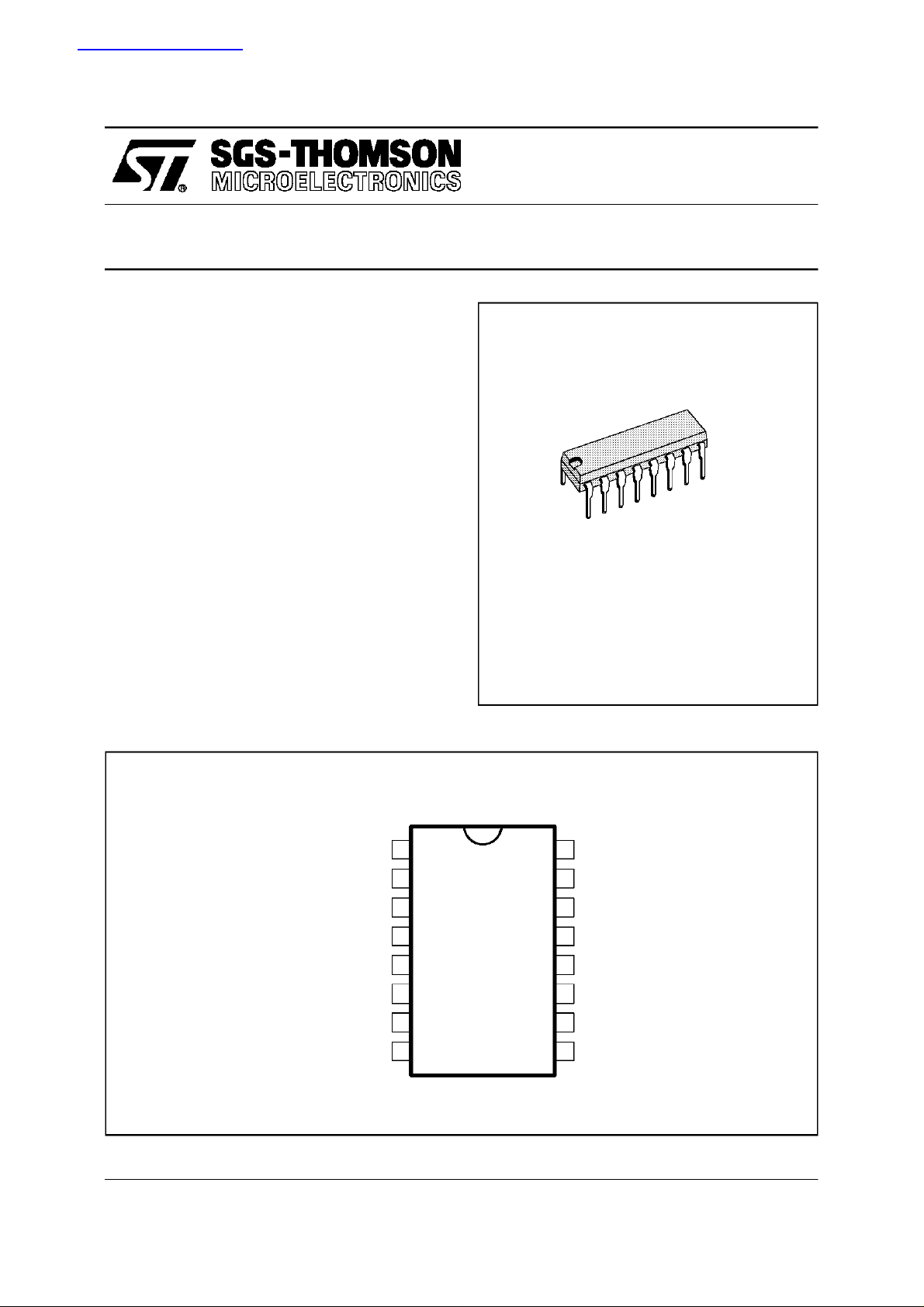
The TDA1175Pis a monolithicintegrated circuitin
POWERDIP16 plastic package. It is intended for
use in black and white and colour TV receivers.
Low-noise makes this device particularly suitable
for use in monitors.
The functions incorporated are : synchronization
circuit, oscillator and ramp generator,high power
gain amplifier,flybackgenerator,voltageregulator.
PINCONNECTIONS
RAMPOUTPUT
SUPPLYVOLTAGE
FLYBACK
GROUND
GROUND
POWERAMPLIFIER OUTPUT
POWERAMPLIFIER
SUPPLYVOLTAGE
REGULATED VOLTAGE
1
2
3
4
5
6
7
8
POWERDIP16
(Plastic Package)
ORDER CODE : TDA1175P
16
15
14
13
12
11
10
RAMPGENERATOR
COMPENSATION
AMP. INPUT
GROUND
GROUND
OSCILLATOR
SYNC.INPUT
9
HEIGHTADJUSTMENT
August 1995
1175P-01.EPS
1/8
TDA1175P
BLOCK DIAGRAM
C4 D
+V
S
A
SYNC
FREQ
C1
P1
11
10
TDA1175P
OSCILLATOR
CIRCUIT
SYNC
125413
TABS
HEIGHT
8
VOLTAGE
REGULATOR
RAMP
GENERATOR
916114
C
A
2
2
FLYBACK
GENERATOR
BUFFER
STAGE
LINEARITY
P3P2 R
C3
37
PREAMPLIFIER
R
B
POWER
AMPLIFIER
6
R
G
15
R
D
R
C
C6
R
H
C8
ABSOLUTEMAXIMUMRATINGS
Symbol Parameter Value Unit
V
V
6,V7
V
I
I
I
I
I
I
P
T
stg,Tj
s
14
o
o
o
3
3
10
tot
Supply Voltage at Pin 2 35 V
Flyback Peak Voltage 60 V
Power Amplifier Input Voltage + 10
– 0.5
Output Peak Current (non repetitive)at t =2ms 2 A
Output Peak Current at f = 50Hz, t ≤ 10µs
Output Peak Current at f= 50Hz, t > 10µs
Pin 3 DC Current at V6<V
Pin 3 Peak to Peak Flyback Currentfor f = 50Hz, t
2
≤ 1.5ms
fly
Pin 10 Current ±
Power Dissipation : at T
=90°C
tab
=70°C (freeair) (1)
at T
amb
2.5 A
1.5 A
100 mA
1.8 A
20
4.3
1
Storage and Junction Temperature – 40,+ 150 °
C9
YOKE
C7C5
R
E
R
F
1175P-02.EPS
V
V
mA
W
W
C
1175P-01.TBL
THERMAL DATA
Symbol Parameter Value Unit
R
th (j-tab)
R
th (j-amb)
(1) Obtained with tabs soldered to printed circuit with minimized copper area.
2/8
Thermal Resistance Junction-pin Max. 12
Thermal Resistance Junction-ambient Max. 80 °
°C/W
C/W
(1)
1175P-02.TBL
TDA1175P
ELECTRICALCHARACTERISTICS (T
=25°C,unless otherwisespecified)
amb
Symbol Parameter Test Conditions Min. Typ. Max. Unit Fig.
DC CHARACTERISTICS (Refer to the test circuits, VS= 35V)
I
2
I
7
–I
–I
–I
–I
∆I
16
I
16
V
V
V
V
V
6L
V
6H
V
V
|∆V
|
8
,
∆V
S
V
14
AC CHARACTERISTICS (Refer to the AC test circuit, V
I
s
I
10
V
t
fly
V
ON
f
o
Pin 2 Quiescent Current I3=0 7 14 mA 1b
Pin 7 Quiescent Current I6=0 8 17 mA 1b
Oscillator BiasCurrent V11= 1V 0.1 1 µ
11
Amplifier InputBias Current V14=1V 1 10
14
Ramp Generator Bias Current V16= 0 0.02 0.3 µ
16
Ramp Generator Current
16
Ramp Generator Non-linearity
Supply VoltageRange 10 35 V
s
Pin 1 Saturation Voltage to Ground I1= 1mA 1 1.4 V
1
Pin 3 Saturation Voltage to Ground I3= 10mA 1.5 2.5 V 1a
3
Qiuescent output Voltage
6
Output Saturation Voltage to
Ground
=20µA, V16=0
I
9
= 0 to 12V, I9=20µA
∆V
16
= 10V, R1 = 1kΩ,R2=1kΩ
V
s
V
= 35V, R1 = 3kΩ,R2=1kΩ
s
–I6= 0.1A
= 0.8A
–I
6
Output Saturation Voltage to Supply I6= 0.1A
= 0.8A
I
6
Regulated Voltageat Pin8 6.5 6.7 6.9 V 1b
8
Regulated Voltageat Pin9
9
Regulated VoltageDrift with Supply
|∆V
|
9
Voltage
∆V
S
Amplifier InputReference Voltage
Supply Current Iy=1A
=20µA
I
9
∆Vs = 10 to 35V
≤ 0.4V
V
10
= 22V, f =50Hz)
S
PP
Sync. Input Current (positive or
18.5 20 21.5
0.2 1 % 1b
4.1
4.4
8.2
4.7
8.8
9.4VV1a1a
0.9
1.2
1.8
2.2Vv1c1c
1.4
2.1
2.8
3.1VV1d1d
6.6 6.8 7 V 1b
1 2 mV/V 1b
2.20 2.27 2.35 V
140 mA 2
0.5 2 mA 2
negative)
Flyback Voltage Iy=1A
6
Flyback Time Iy=1A
PP
PP
45 V 2
0.7 ms 2
Peak to PeakOutput Noise Pin 11 Connected to GND 18 30 mVpp 2
Free Running Frequency
(P1 + R1) =300kΩ
36 43.5 Hz 2
A
µA
A
µA
C9 = 0.1 µF
f
OPER
∆f
Operating Frequency Range 10 120 Hz 2
Synchronization Range
= 0.5mA, C9 = 0.1µF
I
10
14 Hz 2
(P1+R1) = 300kΩ
∆f
∆V
|∆f
∆T
Frequency Drift with Supply Voltage Vs= 10 to 35V 0.005 Hz/V 2
S
|
Frequency Drift with tab
Temperature
ab
= 40 to 120°C
T
tab
0.01
Hz/°C
1a
1b
1a
1b
2
1175P-03.TBL
3/8

TDA1175P
Figure1 : DC Test Circuits
Figure1a
V
3
10
11
I
8
1kΩ
1V 1V 8V
-I -I
9
Figure1c
+V
I
3
3
S
7
2
TDA1175P
916 14
TABS
12
R2
+V
S
6
R1
V
4
Figure1b
1175P-03.EPS
Figure1d
+V
I
2
S
I
5
27
11
6
TDA1175P
16
-I
12
14
98
TABS
V
7
100kΩ
+V
S
-IV
10
1V
1175P-04.EPS
11
27
TDA1175P
14
4V
TABS
I
4
6
V
4L
11
27
TDA1175P
14
TABS
6
V
4H
I
4
1V
1175P-05.EPS
1175P-06.EPS
4/8

TDA1175P
Figure2 : ACTest and Application Circuit for LargeScreen B/WTV Set 10Ω/20mH/1A
V = 22V
0.1µF
100µF
SYNC.
INPUT
P1
100kΩ
1N4001
TABS
7
36
10
TDA1175P
470µF
2
3.3Ω
220kΩ
15
470pF
0.1µF
100pF
5.6kΩ
14
22kΩ
1
11
R1
220kΩ
89
100kΩ
16
100kΩ
47kΩ
1.8kΩ
5.6kΩ
10µF
S
Yoke
Ry = 10Ω
Ly = 20mH
1000µF
PP
560Ω*
0.1µF
C9
0.1µF
120kΩ
910kΩ
0.1µF
1Ω
* on application only
Figure3 : TypicalApplication Circuit for VGA Monitor (RY=10Ω,LY= 20mH,IY= 0.8APP)
C9 C10 560pF
1175P-07.EPS
V
(26V)
3.3nF
S
3.3kΩ
1.8nF
C2
1000µF
35V
R1
C5
0.15µF
V. FREQ
D1
1N4007
C3
100µF
35V
C4
P1
100kΩ
200kΩ
R3
240kΩ
7
3
10
11
82kΩ
R5
C1
0.1µF
R2
P2
220kΩ
15
8
V. SIZE
R12
220kΩ
2
TDA1175P
9
R4
1MΩ
6
16
45
C6
0.1µF
C7
0.1µF
R13
3.3Ω
C11
0.1µF
12 13
14
1
22µF
50kΩ
V.LIN
56kΩ
35V
P3
R6
R11
2.7kΩ
C8
R7
27kΩ
R8
47kΩ
R10
0.82Ω
R14
220Ω
1/2W
R9
5.1kΩ
C12
470µF
50V
Y1
YOKE
1175P-08.EPS
5/8

TDA1175P
Figure4 : P.C. Board andComponents Layoutof the Circuit of Figure3 (1:1 scale)
C9
C12
R14
C18
R18
R11
C11
R10
Y1
R8
R7
C7
BILL OF MATERIAL
Item Qty Reference Part
1 4 C1, C6, C7, C11
21 C2
31 C3
41 C4
5 1 C5 1.8nF
61 C8
7 1 C9 3.3nF
8 1 C10 560pF
9 1 C12
10 1 D1 1N4007
11 1 IC1 TDA1175P
12 1 P1
13 1 P2
14 1 P3
15 1 R1
1000µF 35V
100µF 35V
0.15µF
22µF 35V
470µF 50V
100kΩ POT
220kΩ POT
50kΩPOT
C4
C8
R4
0.1µF
3.3kΩ
R12
V-FREQ
C6
V-SIZE
P1
IC1
R8
P2
R6C2R9
R2
GND
R1
D1
R6
C1
C3
P3
V.LIN
R
C6
VS
1175P-09.EPS
Item Qty Reference Part
16 1 R2
17 1 R3
18 1 R4
19 1 R5
20 1 R6
21 1 R7
22 1 R8
23 1 R9
24 1 R10
25 1 R11
26 1 R12
27 1 R13
28 1 R14
29 1 Y1 YOKE
82kΩ
240kΩ
1MΩ
200kΩ
56kΩ
27kΩ
47kΩ
5.1kΩ
0.82Ω
2.7kΩ
220kΩ
3.3Ω
220Ω 1/2W
1175P-04.TBL
6/8

MOUNTINGINSTRUCTION
The R
canbe reducedby soldering the GND
th (j-a)
pins to a suitablecopper area of theprinted circuit
board (Figure 5) or to an external heatsink (Figure 6).
The diagram of Figure 7 shows the maximum
dissipablepower P
and the R
tot
as a function
th (j-a)
of the side ”I” of two equal square copper areas
Figure 5 : Exampleof P.C.BoardCopper Area
TDA1175P
having a thicknessof35µ (1.4 mils).
During soldering the pins temperature must not
exceed260°C and the solderingtime must not be
longerthan 12 seconds.
Theexternalheatsinkor printedcircuitcopperarea
mustbe connectedto electricalground.
Figure6 : ExternalHeatsink Mounting Example
Figure 7 : Maximum PowerDissipation and
Junction-ambientThermal
Resistanceversus ”I”
1175P-10.EPS
Figure8 : Maximum AllowablePower Dissipation
versus Ambient Temperature
1175P-12.EPS
1175P-11.EPS
1175P-13.EPS
7/8

TDA1175P
PACKAGE MECHANICAL DATA
16 PINS- PLASTICPOWERDIP
I
L
b1
E
Dimensions
a1
Z
b
16
18
B
e3
D
e
9
F
Millimeters Inches
Min. Typ. Max. Min. Typ. Max.
a1 0.51 0.020
B 0.85 1.4 0.033 0.055
b 0.5 0.020
b1 0.38 0.5 0.015 0.020
D 20 0.787
E 8.8 0.346
e 2.54 0.100
e3 17.78 0.700
F 7.1 0.280
i 5.1 0.201
L 3.3 0.130
Z 1.27 0.050
PMDIP16W.EPS
DIP16PW.TBL
Information furnished is believed tobe accurate and reliable. However,SGS-THOMSON Microelectronics assumesno responsibility
for the consequences of use of suchinformation nor forany infringementof patents or other rights of thirdparties which may result
from its use. No licenceisgranted by implication or otherwise under anypatent orpatent rights ofSGS-THOMSON Microelectronics.
Specifications mentioned in this publication are subject to change without notice. This publication supersedes and replaces all
information previously supplied. SGS-THOMSON Microelectronics products are notauthorized for use as critical componentsin life
support devicesor systems without express written approval of SGS-THOMSON Microelectronics.
1995 SGS-THOMSON Microelectronics - AllRights Reserved
Purchase of I
2
I
C Patent.Rights to usethese components in a I2C system,is granted provided that the system conforms to
Australia -Brazil - China - France - Germany - Hong Kong - Italy - Japan - Korea - Malaysia - Malta - Morocco
The Netherlands- Singapore - Spain - Sweden - Switzerland -Taiwan - Thailand- United Kingdom - U.S.A.
2
C Components of SGS-THOMSON Microelectronics, conveys a licenseunder the Philips
2
the I
C Standard Specifications as defined by Philips.
SGS-THOMSON Microelectronics GROUP OF COMPANIES
8/8
 Loading...