

查询TDA1170N供应商
LOW-NOISE TV VERTICALDEFLECTIONSYSTEM
.
COMPLETEVERTICAL DEFLECTION
SYSTEM
.
LOW NOISE
.
SUITABLE FOR HIGH DEFINITION
MONITORS
TDA1170N
DESCRIPTION
The TDA1170Nis a monolithicintegratedcircuit in
a 12-lead quad in-line plastic package. It is intended for use in black and white and colour TV
receivers.Low-noisemakesthis deviceparticularly
suitable for usein monitors.The functionsincorporated are : synchronization circuit, oscillator and
ramp generator,high power gain amplifier, flyback
generator,voltage regulator.
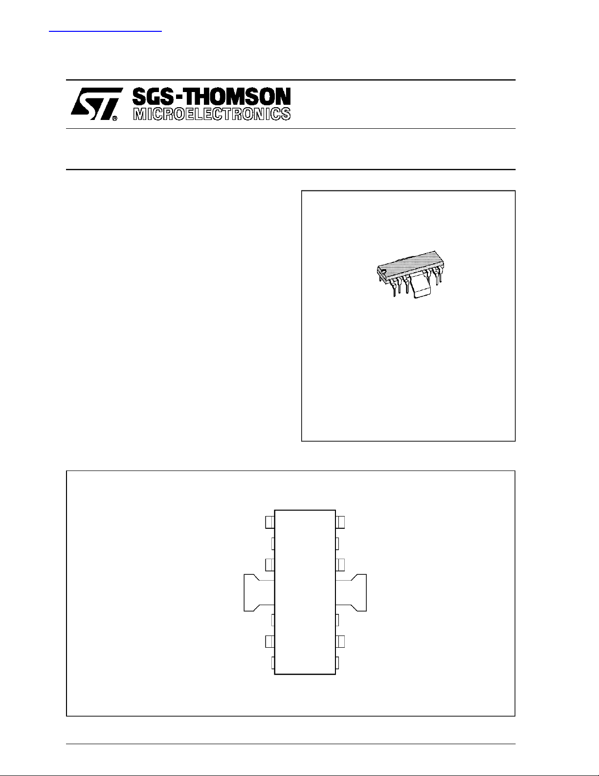
PIN CONNECTIONS
RAMP OUTPUT
SUPPLY VOLTAGE
FLYBACK
GROUND
FINDIP12
(Plastic Package)
ORDER CODE : TDA1170N
1 12 RAMP GENERATOR
2
3
11
10
COMPENSATION
AMP. INPUT
GROUND
POWER AMPLIFLIER OUTPUT
December 1992
POWER AMPLIFLIER
SUPPLY VOLTAGE
REGULATED
VOLTAGE
4
5
67
9
8
OSCILLATOR
SYNC. INPUT
HEIGHT ADJUSTMENT
1170N-01.EPS
1/8
TDA1170N
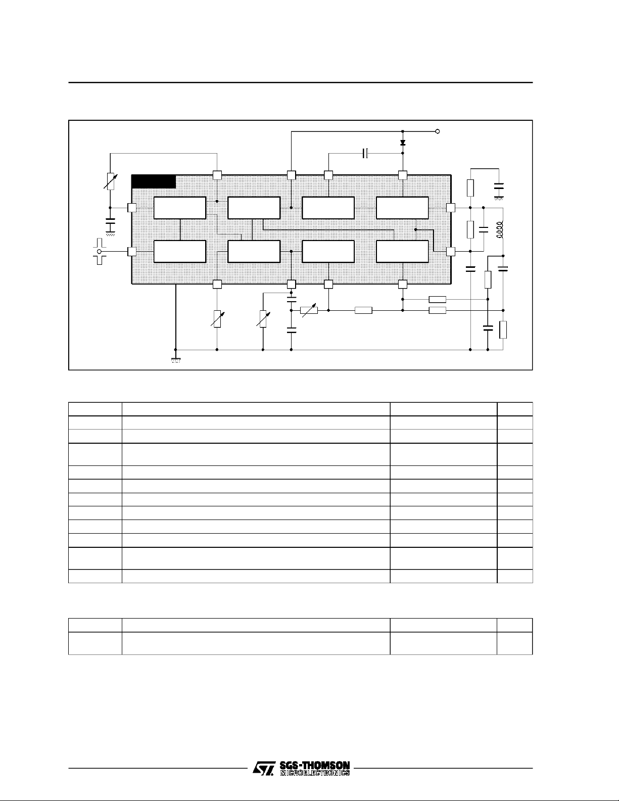
BLOCK DIAGRAM
C
4
D
A
+V
S
FREQ
SYNC
P
TDA1170N
1
9
OSCILLATOR
C
1
TABS
SYNC
CIRCUIT
8
6
VOLTAGE
REGULATOR
RAMP
GENERATOR
712110
HEIGHT
2
2
LINEARITY
C
2
R
A
35
FLYBACK
GENERATOR
BUFFER
STAGE
PP
3
C
3
AMPLIFLIER
PREAMPLIFLIER
R
B
POWER
R
H
4
R
G
C
8
11
57
R
D
R
C
C
6
ABSOLUTEMAXIMUM RATINGS
Symbol Parameter Value Unit
V
V
4,V5
V
I
I
I
I
I
I
P
T
stg,Tj
S
10
o
o
o
3
3
8
tot
Supply Voltage at Pin 2 35 V
Flyback Peak Voltage 60 V
Power Amplifier Input Voltage + 10
– 0.5
Output Peak Current (non repetitive) at t = 2msec 2 A
Output Peak Current at f = 50Hz t ≤ 10µsec 2.5 A
Output Peak Current at f = 50Hz t > 10µsec 1.5 A
Pin 3 DC Current at V4<V
2
Pin 3 Peak to Peak Flyback Current for f = 50Hz, t
≤ 1.5msec 1.8 A
fly
100 mA
Pin 8 Current ± 20 mA
Power Dissipation : at Tab=90°C
=80°C (freeair)
at T
amb
5
1
Storage and Junction Temperature – 40, +150 °C
C
9
YOKE
CC
R
E
R
F
1170N-02.EPS
V
V
W
W
1170N-01.TBL
THERMALDATA
Symbol Parameter Value Unit
R
th j-tab
R
th j-amb
Thermal Resistance Junction-tab
Thermal Resistance Junction-ambient
* Obtained with tabs soldered to printed circuit with minimized copper area.
2/8
Max
Max
12
70
°C/W
°C/W *
1170N-02.TBL
TDA1170N
ELECTRICALCHARACTERISTICS
(Refer to the test circuits, V
=35V, T
S
DC CHARACTERISTICS
Symbol Parameter Test Conditions Min. Typ. Max. Unit Fig.
I
2
I
5
–I
–I
–I
–I
∆I
12
I
12
V
V
1
V
3
V
4
V
4L
V
4H
V
6
V
7
|
|∆V
6
;
∆V
S
V
10
R8 Pin 8 Input Resistance V
Pin 2 Quiescent Current I3=0 7 14 mA 1b
Pin 5 Quiescent Current I4=0 8 17 mA 1b
Oscillator Bias Current V9= 1V 0.1 1 µA1a
9
Amplifier Input Bias Current V10=1V 1 10 µA1b
10
Ramp Generator Bias Current V12= 0 0.02 0.3 µA1a
12
Ramp Generator Current I7=20µA, V12= 0 18.5 20 21.5 µA1b
12
Ramp Generator Non-linearity ∆V12 = 0 to 12V, I7=20µA 0.2 1 % 1b
Supply Voltage Range 10 35 V
s
Pin 1 Saturation Voltage to Ground I1= 1mA 1 1.4 V
Pin 3 Saturation Voltage to Ground I3= 10mA 300 450 mV 1a
Qiuescent output Voltage VS= 10V
Output Saturation Voltage to Ground – I4= 0.1A
Output Saturation Voltage to Supply I4= 0.1A
Regulated Voltage at Pin 6 6.1 6.5 6.9 V 1b
Regulated Voltage at Pin 7 I7=20µA 6.2 6.6 7 V 1b
∆V
7
Regulated Voltage Drift with Supply
Voltage
∆V
S
Amplifier Input Reference Voltage 2.07 2.2 2.3 V
=25oC,unless otherwisespecified)
amb
R1= 1kΩ,R2=1kΩ
V
= 35V
S
R1= 3kΩ,R2=1kΩ
= 0.8A
–I
4
= 0.8A
I
4
= 10 to 35V 1 mV/V 1b
∆V
S
≤ 0.4V 1 MΩ 1a
8
4.1 4.4 4.75 V 1a
8.3 8.8 9.45 V 1a
0.9
1.2
1.9
2.3VV
1.4
2.1
2.8
3.2VV
1c
1c
1d
1d
1170N-03.TBL
3/8

TDA1170N
Figure 1 : DCTestCircuits
Figure1a
I8
1kΩ
1V 1V 8V
Figure1c
V3 I3
8
9
712
+Vs
32
TDA1170N
TABS
- I12-I9
+Vs
5
4
10
R2
Figure1b
I2
2
910
R1
6
V4
V6
- I12
TDA1170N
12
7
V7
100kΩ
1170N-03.EPS
+Vs
I5
5
TABS
- I10
1V
1170N-04.EPS
Figure1d
+Vs
2
94
TDA1170N
10
4V
TABS
5
I4
2
TDA1170N
10
V4L
1170N-05.EPS
1V
TABS
5
V4H
49
I4
1170N-06.EPS
4/8

TDA1170N
ELECTRICAL CHARACTERISTICS
(Refer to the AC test circuit,V
= 22V ; f = 50Hz ; T
S
AC CHARACTERISTICS
Symbol Parameter Test Conditions Min. Typ. Max. Unit
Supply Current Iy= 1App 140 mA
I
s
Sync. Input Current (positive or negative) 500 µA
I
8
V4 Flyback Voltage I
t
V
Flyback Time Iy= 1App 0.7 ms
fly
Peak to Peak Output Noise Pin 9 Connected to GND 40 mV
ON
f
Free Running Frequency (P1 + R1) = 300kΩ, C2 = 0.1µF
o
∆f Sychronization Range I
∆f
∆V
| ∆f|
∆T
Frequency Drift with Supply Voltage Vs= 10 to 35V 0.005 Hz/V
S
Frequency Drift with tab Temperature T
ab
Figure2 : AC Test and ApplicationCircuitfor Large Screen B/W TV Set 10Ω/20mH/1App
1N4001
=25°C, unless otherwise specified)
amb
= 1App 45 V
y
42.2
(P1 + R1) = 260kΩ, C2 = 0.1µF
= 0.5mA 14 Hz
8
= 40 to 120°C 0.01 Hz/°C
tab
V = 2.2V
S
470µF
48.5
PP
Hz
Hz
1170N-04.TBL
0.1µF 100µF
Sync.
Input
C2
P1
0.1µF
TABS
52
3
T
D
A
8
1
1
7
0
N
9
76
R1
100kΩ
120kΩ
4
11
10
1
910kΩ
0.1µF
0.1µF
100k
220k
470pF
22kΩ
Ω
3.3Ω
Ω
47kΩ
100pF
5.6kΩ
1.8kΩ
0.1µF
5.6kΩ
µ
YOKE
Ry = 10Ω
Ly = 20mH
1000µF
1
Ω
1170N-07.EPS
5/8

TDA1170N
Figure 3 : TypicalApplication Circuitfor SmallScreen 90°TVC Set (RY=15Ω,LY=30mH, IY= 0.82 App)
V = 26V
D1
1N4001
C5
470µF
S
C1
0.1µF100µF
f sync=
50Hz
C4
C2
0.1µF
R1
4.7kΩ
P1
C3
0.15µF
52
3
8
9
100k
Ω
R2
150kΩ
P2
100kΩ
R3
T
D
A
1
1
7
0
N
TABS
1276
R4
680kΩ100kΩ
4
10
1
P3
100kΩ
C7
0.1µF
C8
µF
0.1
R8
3.3
Ω
R5 C9
390kΩ
C6
470pF
R6
18kΩ
R7
47kΩ
100pF
R11
5.6kΩ
R10
5.6k
R9
1.5kΩ
C10
0.1µF
R13
270Ω
Ω
C11
10µF
Figure 4 : P.C. Boardand ComponentsLayout of the Circuit of fig. 3 (1:1 scale)
YOKE
Ry = 15Ω
Ly= 30mH
C12
1000µF
R12
1Ω
1170N-08.EPS
6/8
1170N-09.TIF
MOUNTINGINSTRUCTION
During soldering the tab temperature must not
exceed 260°Cand the soldering time must not be
longer than 12 seconds.
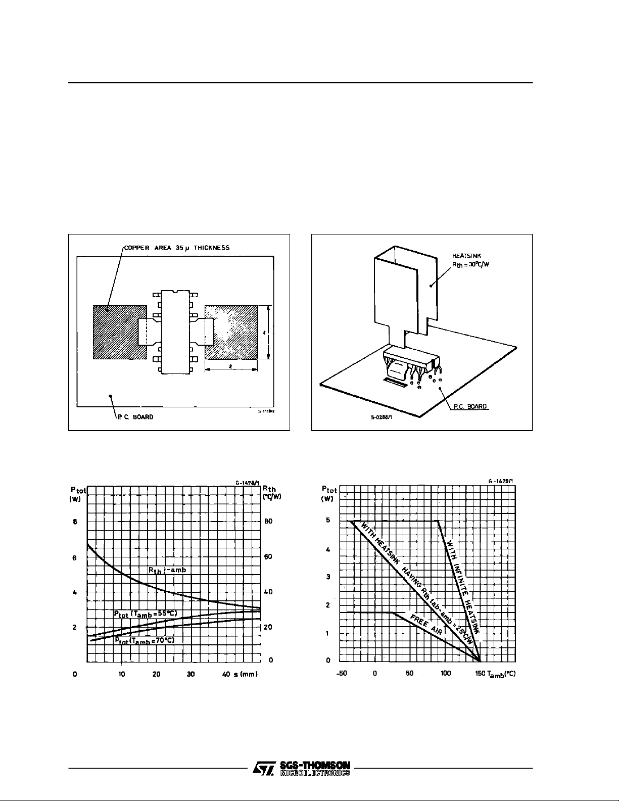
The externalheatsinkor printedcircuitcopperarea
must be connectedto electricalground.
The junctionto ambientthermal resistancecan be
Figure 5 : Exampleof P.C. Board Copper Area
Used as Heatsink
TDA1170N
reducedby solderingthe tabs to a suitable copper
area of the printed circuit board (fig. 5) or to an
externalheatsink(fig. 6).
The diagramof fig. 7 shows the maximum dissipable power P
and the R
tot
side ”e” of two equal square copper areas having
a thicknessof35 µ (1.4 mil).
Figure6 : Example of Externalheatsink
as a function of the
th j-amb
Figure 7 : MaximumPowerDissipation and
Junction-AmbientThermal
Resistanceversus ”e”
1170N-10.EPS
Figure8 : MaximumAllowable Power
DissipationversusAmbient
Temperature
1170N-12.EPS
1170N-11.EPS
1170N-13.EPS
7/8

TDA1170N
PACKAGE MECHANICAL DATA : 12 PINS - PLASTIC FINDIP
G
e4
b1
E1
E2
E
Dimensions
D
AL
I
a1
b
c1
12
16
e5
c
e6
e3
K
D
e
7
M
F
Millimeters Inches
Min. Typ. Max. Min. Typ. Max.
A 3.8 4.05 0.150 0.159
a1 1.5 1.75 0.059 0.069
b 0.55 0.6 0.022 0.024
b1 0.3 0.35 0.012 0.014
c 1.32 0.052
c1 0.94 0.037
D 19.2 19.9 0.756 0.783
E 16.8 17.2 17.6 0.661 0.677 0.693
E1 4.86 5.56 0.191 0.219
E2 10.11 10.81 0.398 0.426
e 2.29 2.54 2.79 0.090 0.100 0.110
e3 17.43 17.78 18.13 0.686 0.700 0.714
e4 7.62 0.300
e5 7.27 7.62 7.97 0.286 0.300 0.314
e6 12.35 12.7 13.05 0.486 0.500 0.514
F 6.3 7.1 0.248 0.280
G 9.8 0.386
I 7.8 8.6 0.307 0.339
K 6.1 6.5 0.240 0.256
L 2.5 2.9 0.098 0.114
M 2.5 3.1 0.098
Information furnishedis believed to be accurateand reliable. However, SGS-THOMSON Microelectronics assumes no responsibility
for the consequences of use of such information nor for anyinfringement of patents or other rights of third partieswhichmay result
from its use. No licence is granted by implication or otherwise underany patent or patent rights of SGS-THOMSON Microelectronics.
Specifications mentioned in this publication are subject to change without notice. This publication supersedes and replaces all
information previouslysupplied. SGS-THOMSON Microelectronics products are not authorized for use as critical components in life
support devices or systems without express written approval of SGS-THOMSON Microelectronics.
PM-FDIP.EPS
FINDIP.TBL
8/8
1994 SGS-THOMSON Microelectronics - All Rights Reserved
Purchase of I2C Components of SGS-THOMSON Microelectronics, conveys a license under the Philips
2
I
C Patent. Rights to use these components in a I2C system, is granted provided that the system conforms to
2
the I
C Standard Specifications as defined by Philips.
SGS-THOMSON Microelectronics GROUP OF COMPANIES
Australia - Brazil - China - France - Germany - Hong Kong - Italy - Japan - Korea - Malaysia - Malta - Morocco
The Netherlands - Singapore - Spain - Sweden - Switzerland - Taiwan - Thailand - United Kingdom - U.S.A.
 Loading...