

SGS-THOMSON STH60N10, STH60N10FI, STW60N10 Technical data
查询STH60N10供应商
STH60N10/FI
STW60N10
N - CHANNEL ENHANCEMENT MODE
POWER MOS TRANSISTOR
TYPE V
STH 60N10
STH 60N10FI
STW60N10
■ TYPICAL R
■ AVALANCHE RUGGED TECHNOLOGY
■ 100% AVALANCHE TESTED
■ REPETITIVE AVALANCHE DATA AT 100
■ LOW GATE CHARGE
■ VERY HIGH CURRENT CAPABILITY
o
■ 175
■ APPLICATION ORIENTED
C OPERATING TEMPERATURE
DS(on)
DSS
100 V
100 V
100 V
= 0.02 Ω
R
DS(on)
< 0.025 Ω
< 0.025 Ω
< 0.025 Ω
I
D
60 A
36 A
60 A
o
C
CHARACTERIZATION
APPLICATIONS
■ HIGH CURRENT, HIGH SPEED SWITCHING
■ SOLENOID AND RELAY DRIVERS
■ REGULATORS
■ DC-DC & DC-AC CONVERTERS
■ MOTOR CONTROL, AUDIO AMPLIFIERS
■ AUTOMOTIVE ENVIRONMENT (INJECTION,
ABS, AIR-BAG, LAMPDRIVERS, Etc.)
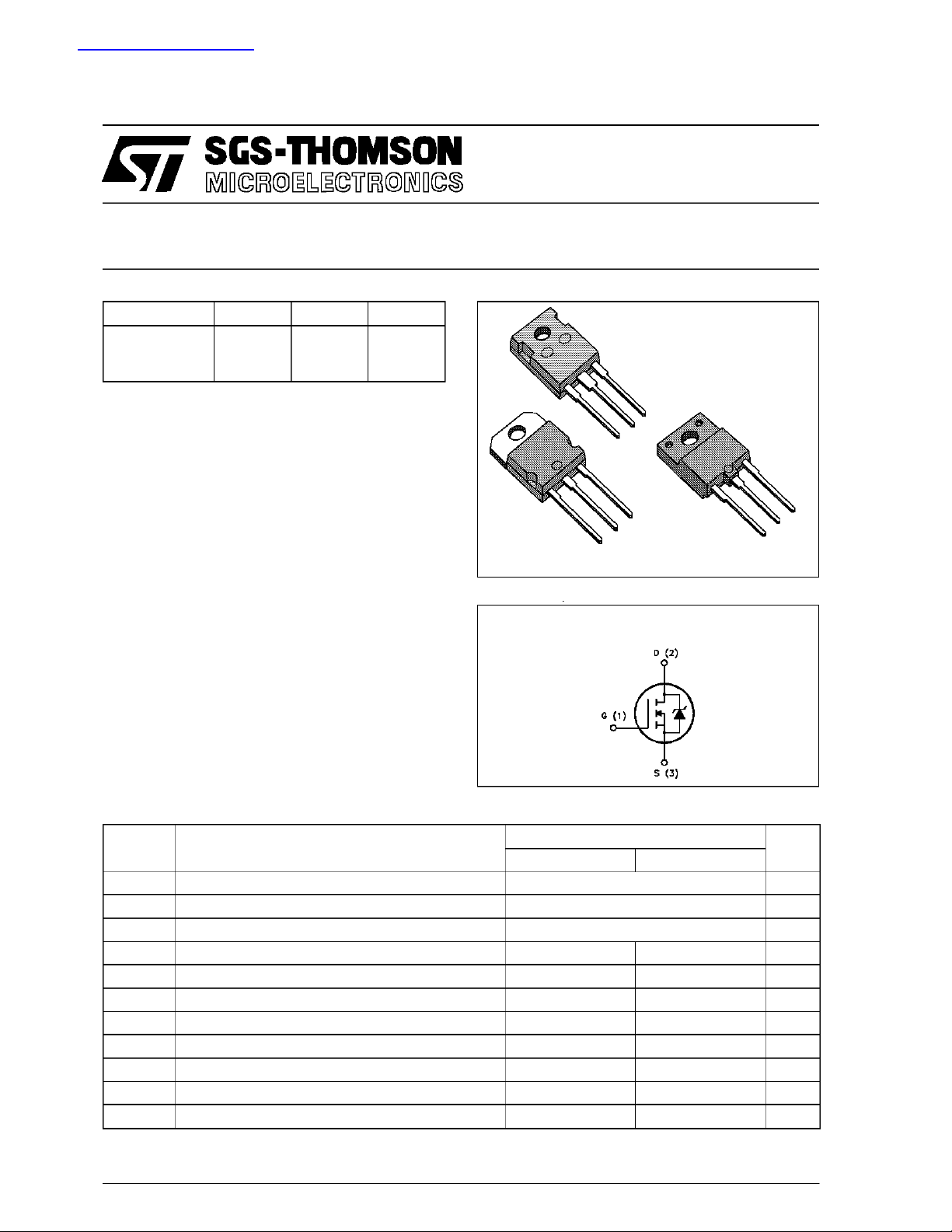
TO-247
3
2
1
3
2
TO-218 ISOWATT218
1
INTERNAL SCHEMATIC DIAGRAM
3
2
1
ABSOLUTE MAXIMUM RATINGS
Symb o l Paramet er Val u e Unit
STH/STW60N10 STH6 0N10FI
V
V
V
I
DM
P
V
T
(•) Pulsewidth limited bysafe operating area
May 1993
Drain - s ource Voltage (VGS=0) 100 V
DS
Drain- gate Voltage (RGS=20kΩ)100V
DGR
Gate-source Voltage ± 20 V
GS
Drain Current (continuous) at Tc=25oC6036A
I
D
Drain Current (continuous) at Tc=100oC42 22A
I
D
(•) Drain Current (pulsed) 240 240 A
Total Di ssipation at Tc=25oC 200 70 W
tot
Derat ing Factor 1.33 0.56 W/
Ins ulation Withs t and Voltage (DC) 4000 V
ISO
St or a ge Tem perature -65 to 175 -65 to 1 50
stg
Max. Operating Junction Temperature 175 1 50
T
j
o
o
o
C
C
C
1/11
STH60N10/FI STW60N10
THERMAL DATA
TO - 218/ TO-247 IS OWATT218
R
thj-case
R
thj-amb
R
thc-sink
T
AVALANCHE CHARACTERISTICS
Symbol Parameter Max Value Uni t
I
AR
E
E
I
AR
Thermal Resistance Junction - cas e Max 0.75 1.79
Thermal Resistance Junction- ambient Max
Thermal Resistance Case-sink Typ
Maximum Lead T emperature For Soldering Purpose
l
Avalanc h e Cu rr ent , Repet itive or Not-R ep et itive
(pulse width limited by Tjmax, δ <1%)
Single Pul se Avalanche Ener gy
AS
(starti ng T
Repetitive Avalanc he Energ y
AR
=25oC, ID=IAR,VDD=25V)
j
(pulse width limited by Tjmax, δ <1%)
Avalanc h e Cu rr ent , Repet itive or Not-R ep et itive
(Tc= 100oC, pulse width limited by Tjmax, δ <1%)
30
0.1
300
60 A
720 mJ
180 mJ
37 A
o
C/W
o
C/W
o
C/W
o
C
ELECTRICAL CHARACTERISTICS (T
=25oC unless otherwise specified)
case
OFF
Symbol Parameter Test Co ndition s Min. Typ. Max. Unit
V
(BR)DSS
Drain - s ource
ID=250µAVGS= 0 100 V
Break d own Volta ge
I
DSS
I
GSS
Zer o Gate Volt age
Drain Current (VGS=0)
Gat e- body Leak age
Current (V
DS
=0)
VDS=MaxRating
VDS= Max Rating x 0 .8 Tc=125oC
= ± 20 V ± 100 nA
V
GS
250
1000µAµA
ON (∗)
Symbol Parameter Test Co ndition s Min. Typ. Max. Unit
V
GS(th)
R
DS(on)
I
D(on)
Gate Threshold Voltage VDS=VGSID=250µA22.94V
St at ic Drain-s our ce O n
Resistance
On State Drain Current VDS>I
VGS=10V ID=30A
VGS=10V ID=30A Tc= 100oC
D(on)xRDS(on)max
0.02 0.025
0.05
60 A
VGS=10V
DYNAMIC
Symbol Parameter Test Co ndition s Min. Typ. Max. Unit
(∗)Forward
g
fs
Tr ansconductance
C
C
C
Input Capacitance
iss
Out put Capacitance
oss
Reverse Transfer
rss
Capacitance
VDS>I
D(on)xRDS(on)maxID
=30A 25 35 S
VDS=25V f=1MHz VGS= 0 4000
1100
250
5000
1400
350
Ω
Ω
pF
pF
pF
2/11
STH60N10/FI STW60N10
ELECTRICAL CHARACTERISTICS (continued)
SWITCHING ON
Symbol Parameter Test Co ndition s Min. Typ. Max. Unit
t
d(on)
(di/dt)
Q
Q
Q
Turn-on T im e
t
Rise Time
r
Turn-on C urrent S lope VDD=80V ID=60A
on
Total Gate Charge
g
Gat e- Source Charge
gs
Gate-Drain Charge
gd
SWITCHING OFF
Symbol Parameter Test Co ndition s Mi n. Ty p. Max. Unit
t
r(Voff)
t
Off -voltage R ise Time
t
Fall Time
f
Cross-over Time
c
SOURCE DRAIN DIODE
VDD=80V ID=30A
RG=50 Ω VGS=10V
90
270
(see test circuit, figure 3)
270 A/µs
RG=50 Ω VGS=10V
(see test circuit, figure 5)
VDD=80V ID=30A VGS=10V 120
16
60
VDD=80V ID=60A
RG=50 Ω VGS=10V
(see test circuit, figure 5)
200
210
410
130
380
170 nC
280
290
570
ns
ns
nC
nC
ns
ns
ns
Symbol Parameter Test Co ndition s Mi n. Ty p. Max. Unit
I
I
SDM
SD
Source-drain Current
(•)
Source-drain Current
60
240
(pulsed)
V
(∗) Forward On Volt age ISD=60A VGS=0 1.6 V
SD
t
Reverse Recovery
rr
Time
Q
Reverse Recovery
rr
ISD= 60 A di/dt = 100 A/µs
VDD=30V Tj=150oC
(see test circuit, figure 5)
180
1
Charge
I
RRM
Reverse Recovery
11
Current
(∗) Pulsed:Pulse duration = 300 µs, dutycycle 1.5 %
(•) Pulse widthlimited by safeoperating area
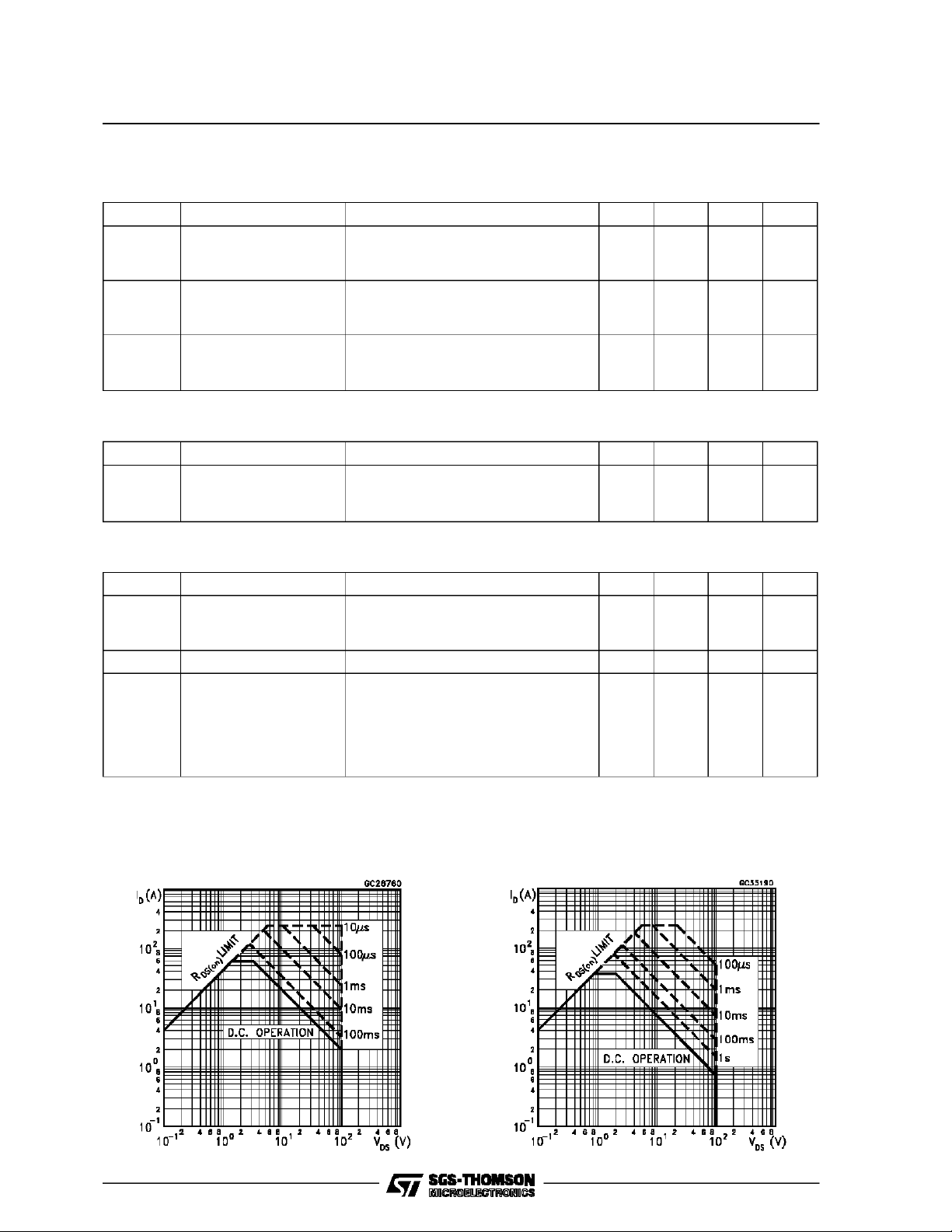
Safe Operating Areas For TO-218 and TO-247 Safe Operating Areas For ISOWATT218
A
A
ns
µC
A
3/11
STH60N10/FI STW60N10
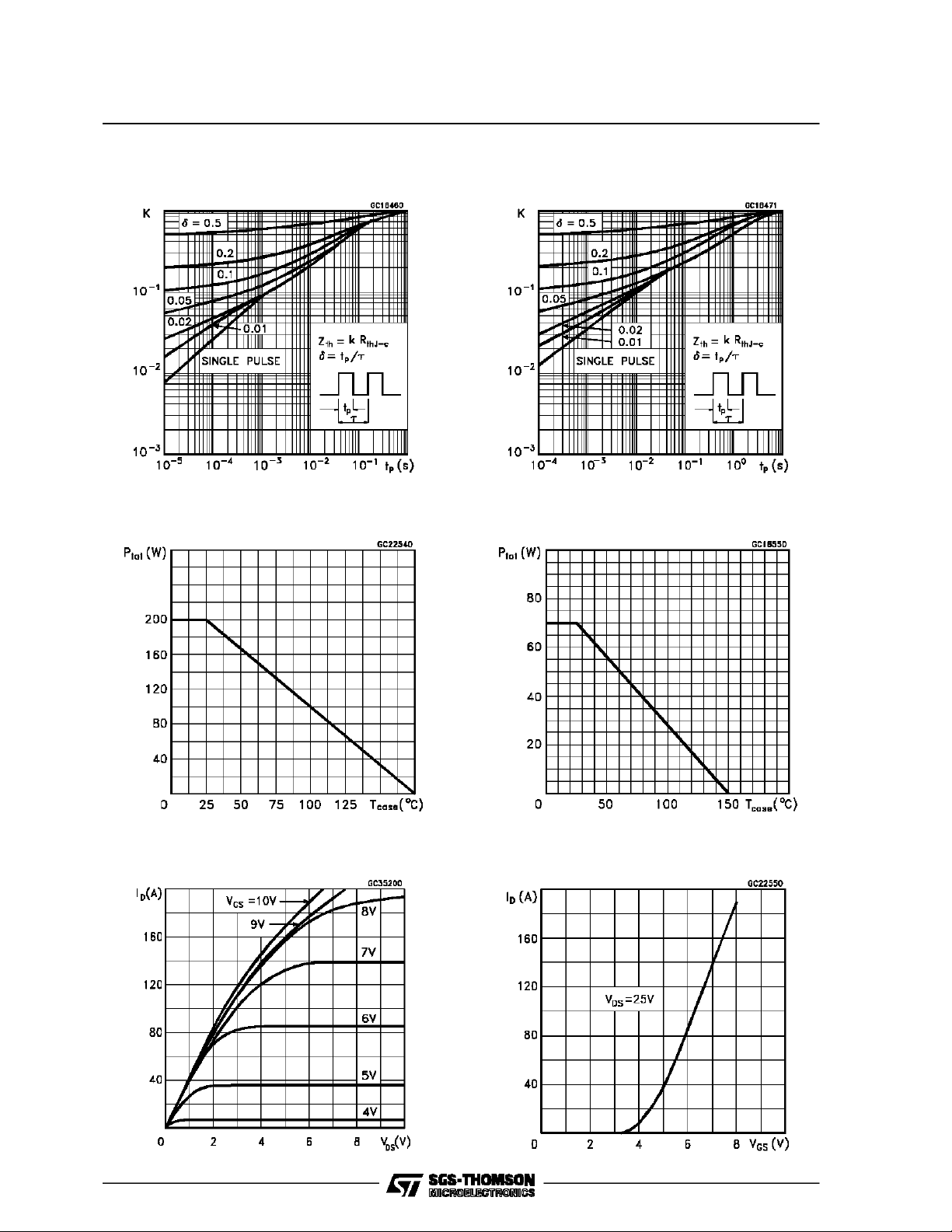
Thermal ImpedeanceFor TO-218 and TO-247
Derating Curve For TO-218 and TO-247
Thermal Impedance For ISOWATT218
Derating Curve For ISOWATT218
Output Characteristics
4/11
Transfer Characteristics
 Loading...