

查询STV8225供应商
.
SOUND AM SYNCHRONOUS DEMODULATOR
.
AM/FMAUDIO SWITCH
.
AV/TVAUDIO SWITCH
.
MUTE INPUT
STV8225
AM SIF CIRCUIT
DESCRIPTION
The STV8225 is intended for the demodulation of
the AM soundof the L standard.
Used as an add on to the STV8224 it permits to
design a multistandard set with the needed
switchesfor one SCART plug.
PINCONNECTIONS
IF INPUT
AGC CAPACITOR
GND
LEVEL SWITCH
FM SOUNDINPUT
1
2
3
4
5
14
13
12
11
10
DIP14
(Plastic Package)
ORDER CODE : STV8225
IF INPUT
MEANCAPACITOR
V
CC
EXTERNALSOUND INPUT
SWITCHINGINPUT
February 1995
MUTE INPUT
MAINSOUNDOUTPUT
6
7
EXTERNALSOUND OUTPUT
9
NOTTO BE CONNECTED
8
8225-01.EPS
1/6
STV8225
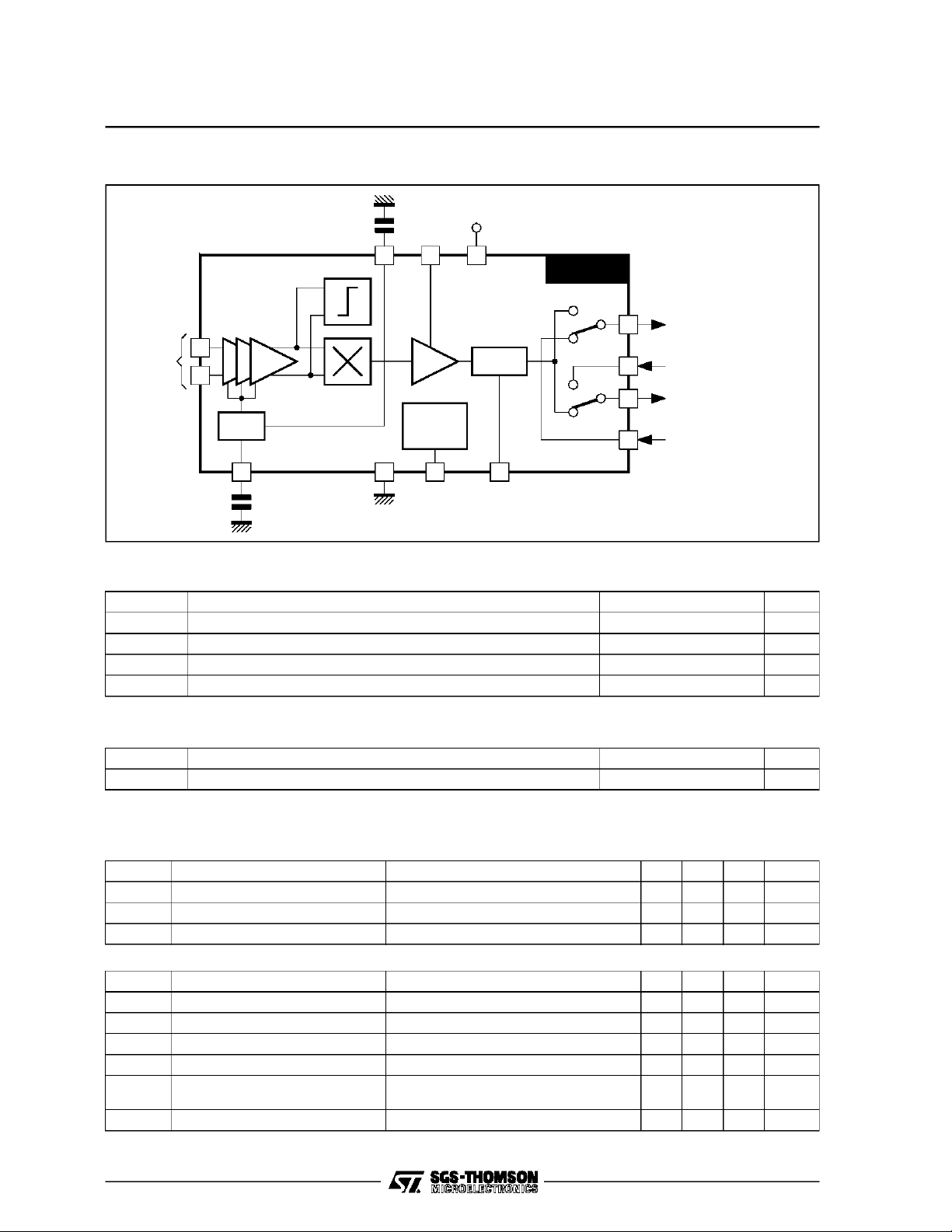
BLOCK DIAGRAM
14
IF INPUT
1
AGC
Mean
Capacitor
Level
Switch
41213
LOGIC
CONT
V
CC
MUTE
STV8225
A
B
SW1
C
A
SW2
7
Main Sound Output
5
FM Sound Input
9
External Sound Output
11
External Sound Input
23
AGC
Capacitor
10
Switching
Input
6
Mute
Input
ABSOLUTEMAXIMUMRATINGS
Symbol Parameter Value Unit
V
CC
T
stg
T
oper
P
tot
Supply Voltage 13 V
Storage Temperature -40, +150
Operating Temperature 0, +70
Power Dissipation 0.35 W
THERMAL DATA
Symbol Parameter Value Unit
R
th (j-a)
ELECTRICAL CHARACTERISTICS (VCC=9V,VIN=10mV
m = 54% modulation depth,Audio BW = 40Hz to 15kHz, T
Symbol Parameter Test Conditions Min. Typ. Max. Unit
V
CC
I
CC
IF AMPLIFIER
Ri 1, 14 Input Resistance (Pins 1-14) Resistancebetween Pin 1 and 14 2 kΩ
Ci 1, 14 Input Capacitance (Pins 1-14) Capacitance between Pin1 and 14 2 pF
VIF min Minimum IF Input Signal IF input signal for V
VIF max Maximum IF Input Signal IF input signal for V
DAV AGC Range DAV = VIF max / VIF min 61 dB
l
AGC
Junction-ambient Thermal Resistance Max. 90
RMS,fSC
amb
=32.4MHz, fM=1kHz,
=25oC, unless otherwisespecified)
Supply Voltage Pin 12 8 9 10 V
Supply Current Pin 12 20 30 mA
Supply Voltage Rejection Pins 9, 7, 12 - V
Maximum AGC Output Current
Charging and discharging ±35 ±50 ±65 µA
= 0.5VPP, f = 100Hz 45 53 dB
Ripple
OUT=VNOM
OUT=VNOM
-3dB 70 µV
+ 1dB 75 mV
(Pin 2)
IF Bandwidth -3dB 50 MHz
o
o
o
C/W
8225-02.EPS
C
C
8225-01.TBL
8225-02.TBL
RMS
RMS
8225-03.TBL
2/6
STV8225
ELECTRICAL CHARACTERISTICS (continued)(VCC=9V,VIN=10mV
m =54% modulation depth, Audio BW = 40Hzto 15kHz, T
=25oC, unless otherwise specified)
amb
RMS,fSC
=32.4MHz, fM=1kHz,
Symbol Parameter Test Conditions Min. Typ. Max. Unit
AM DEMODULATOR
AF Output Voltage(Pins 7-9) Level switch (Pin 4) open
Level switch (Pin 4) connected to GND
AF Bandwidth (Pins 7-9)
-3dB versus nominal signal
Lower Limit
Upper Limit
200
400
50
250
500
300
mV
mV
600
40 Hz
Harmonic Distorsion (Pins 7-9) THD + Noise 0.7 1.8 %
S/N (Pins 7-9) Weighted according to CCIR 468-4 55 dB
MUTE
Threshold Level (Pin 6) Mute mode if voltage below threshold 0.2 0.3 0.4 V
Attenuation (Pins 7-9) Level switch (Pin 4) connected to GND
80 96 dB
TV - AM mode
AUDIO SWITCHES
Switching Voltage (Pin 10) Operation mode
TV
FM
0V V
TV
AM
Viev1
View1 Level 1 (Pin 10) For voltage below this level
AV
AM
Viev2
AV
FM
V
Viev3
CC
10
1.8 2.3 2.6 V
TV-FM mode : Pin 7 connected to A
Pin 9 connected to C
View2 Level 2 (Pin 10) For voltage below this level
4.1 4.6 4.9 V
TV-AM mode : Pin 7 connected to A
Pin 9 connected to A
View3 Level 3 (Pin 10) For voltage below this level
6.4 6.8 7.2 V
AV-AM mode : Pin 7 connected to B
Pin 9 connected to A
For voltage above this level
AV-FM mode : Pin 7 connected to B
Pin 9 connected to C
Input Current (Pin 10) Source current 0.3 2 µA
Input Dynamic Range (Pins 5-11) 2 V
InputResistance (Pins5-11) 35 50 kΩ
Switch Gain V
=2V
IN
Pin 7 vs Pin 11 and Pin 9 vs Pin 5
, f = 1kHz
RMS
-0.6 -0.1 0.4 dB
Crosstalk f = 1kHz 70 85 dB
Output Resistance (Pins7-9) 70 100 130 Ω
Output Current Source (Pins 7-9) 1 mA
Switch Distorsion V
=2V
IN
Pin 7 vs Pin 11 and Pin 9 vs Pin 5
, f = 1kHz, THD+ Noise,
RMS
0.1 0.5 %
Output Noise Unweighted 7 20 µVp
DC Plop at AF Output Pin 10 50 mV
RMS
RMS
kHz
8225-03.EPS
RMS
8225-04.TBL
3/6

STV8225
APPLICATIONDIAGRAM
STV8224- STV8225
External
Sound
Input
Sound
Output
C9
C8
10µF
R11
10µF
220Ω
891011121314
C22
C23
CVBS
Output
Q2
BC547
R18
R12
TRAP FILTER
(5.5MHz - 6.5MHz)
2.2kΩ
(to SCART)
75Ω
L6
R9
560Ω
CF3
8.2µH
Volume
Sound
Output
Switched
R32
C6
4.7µF
10µF
C7
10µF
68nF
Control
10kΩ
C31
100nF
SW1
Mute
1314
CVBS
External
C30
Input
470nF
R29
CVBS
Ouput
75Ω
C27
470nF
+9V
R19
R28
1kΩ
R10
22Ω
+9V
SW4
BC547
STD
R26
3.9kΩ
4.7kΩ
Q3
C11
L7
R25
2.7kΩ
R27
1.8kΩ
R20
1kΩ
1.8kΩ
C24
1nF
R24
4.7kΩ
R21
C26
Level
C12
47µF
100nF
Switch
1617181920 1521222324
100nF
IC1 STV8225
C32
BFP
10nF
D2
CF1
5.5MHz
C28
C17
1µF
C10
22µF
C13
3.3µH
L STD
FILTER
SOUND SAW
IF2
10µF
1234567
L4
C21
3.3µH
BGDKL
FILTER
VIDEO SAW
IF1
C20
47µF
100nF
IC2 STV8224
C19
47nF
1µF
C18
P1
10kΩ
AGC
Tuner
Delay
27kΩ
R14
Q4
LC1
123456789101112
9V
C33
BC337
C25
1µF
38.9MHz
C29
10nF
L5
3.3µH
C14
4.7nF
R13
68Ω
C15
680nF
10µF
DZ1
BZX55C
9V6
1N4148
68pF
Voltage
Switching
BFP
D1
CF2
6.5MHz
1N4148
R22
150Ω
4/6
Tuner AGC
C16
Output
R35
15Ω
R34
47µF
R15
6.8kΩ
12V
390Ω
100kΩ
AFC
R16
Output
100kΩ
8225-06.EPS
R17
9V

INPUT/OUTPUTPINS CONFIGURATION
SC_IN CONTROL SC_OUT
V
CC
10
STV8225
91112
C_MEAN
IF1
IF2
C_AGC
13
14
1
2
2.7V
1kΩ
(charge)
4.2V
I
5kΩ
1kΩ
C
µA
5
V
CC
µA
50µA
125
V
CC
µA
250
µA
250
6.4V
V
REF
4.3V
50kΩ
V
REF
4.3V
10µA
50µA
1mA
100
Ω
V6.4
8
(if used)
1.3kΩ26kΩ
6.0V
µA
125
V
CC
100Ω
7
AUDIO
µA
1mA
250
µA
5
V
CC
50µA
V
6V
CC
V
CC
114kΩ
I
D
(discharge)
100µA
3
GND
4
LSW
50kΩ
V
66kΩ
REF
4.3V
5
FM_IN
10µA
6
STV8225
MUTE
8225-04.EPS
5/6

STV8225
PACKAGE MECHANICAL DATA
14 PINS - PLASTICDIP
Dimensions
Min. Typ. Max. Min. Typ. Max.
Millimeters Inches
a1 0.51 0.020
B 1.39 1.65 0.055 0.065
b 0.5 0.020
b1 0.25 0.010
D 20 0.787
E 8.5 0.335
e 2.54 0.100
e3 15.24 0.600
F 7.1 0.280
i 5.1 0.201
L 3.3 0.130
Z 1.27 2.54 0.050 0.100
Information furnishedis believed to be accurateand reliable. However, SGS-THOMSON Microelectronicsassumes no responsibility
for the consequences of use of such information nor for any infringement of patents or other rights of third partieswhich may result
from its use. No licence is granted by implication or otherwise underany patent or patentrights of SGS-THOMSON Microelectronics.
Specifications mentioned in this publication are subject to change without notice. This publication supersedes and replaces all
information previouslysupplied. SGS-THOMSON Microelectronics products are not authorized for use as critical components in life
support devices or systems without express written approval of SGS-THOMSON Microelectronics.
1995 SGS-THOMSON Microelectronics - All RightsReserved
Purchase of I
2
I
C Patent. Rights to use these components in a I2C system, is granted provided that the system conformsto
Australia - Brazil - China - France - Germany - Hong Kong - Italy - Japan- Korea - Malaysia - Malta - Morocco
The Netherlands - Singapore - Spain - Sweden - Switzerland - Taiwan - Thailand - United Kingdom - U.S.A.
2
C Components of SGS-THOMSON Microelectronics, conveys a license under the Philips
2
the I
C Standard Specifications as defined by Philips.
SGS-THOMSON Microelectronics GROUP OF COMPANIES
PM-DIP14.WMF
DIP14.TBL
6/6

Copyright © Each Manufacturing Company.
All Datasheets cannot be modified without permission.
This datasheet has been download from :
www.AllDataSheet.com
100% Free DataSheet Search Site.
Free Download.
No Register.
Fast Search System.
www.AllDataSheet.com
 Loading...