

SGS-THOMSON STP80N03L-06 Technical data
现货库存、技术资料、百科信息、热点资讯,精彩尽在鼎好!
N - CHANNEL ENHANCEMENT MODE
"ULTRA HIGH DENSITY" POWER MOS TRANSISTOR
TYPE V
DSS
STP80N03L-06 30 V < 0.006 Ω 80 A (*)
R
DS(on)
I
D
STP80N03L-06
TENTATIVE DATA
■ TYPICAL R
■ AVALANCHE RUGGED TECHNOLOGY
■ 100% AVALANCHE TESTED
■ REPETITIVE AVA LANCHE DATA AT 100
■ HIGH CURRENT CAPABILITY
o
■ 175
■ HIGH dV/dt RUGGED NES S
■ APPLICATION ORIENTED
C OPERATING TEMPERATURE
DS(on)
= 0.005 Ω
o
C
CHARACTERIZATION
APPLICATIONS
■ HIGH CURRENT, HIGH SPE ED SWI TCHING
■ POWER MOTOR CONTROL
■ DC-DC & DC-AC CONVERT E RS
■ SYNCRONOUS RECTIFICATION
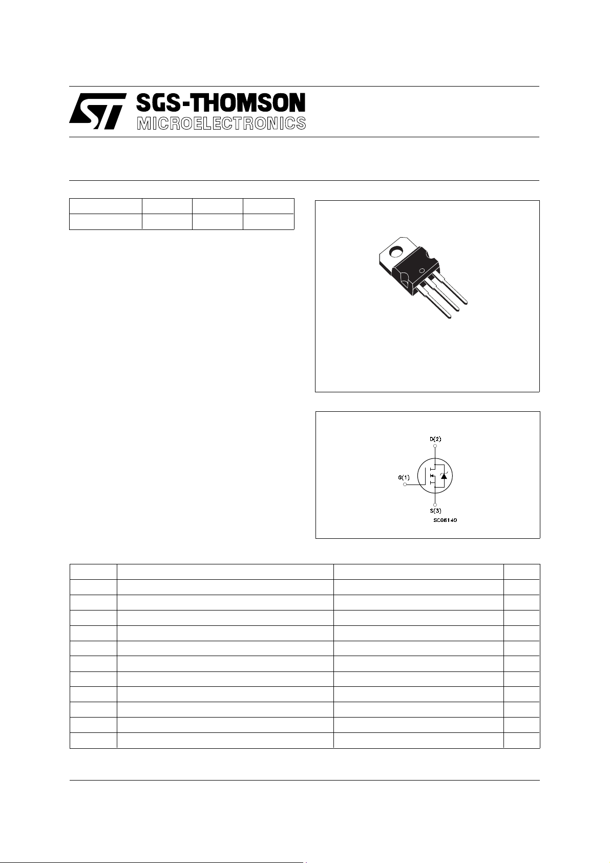
3
2
1
TO-220
INTERNAL SCHEMATIC DIAGRAM
ABSOL UT E MAXIMU M RATINGS
Symbol Parameter Value Unit
V
V
V
I
DM
P
dV/dt(
T
(•) Pulse width limited by safe operating area
March 1996
Drain-source Voltage (VGS = 0) 30 V
DS
Drain- gate Voltage (RGS = 20 kΩ)30V
DGR
Gate-source Voltage ± 15 V
GS
I
Drain Current (continuous) at Tc = 25 oC80A
D
I
Drain Current (continuous) at Tc = 100 oC60A
D
(•) Drain Current (pulsed) 320 A
Total Dissipation at Tc = 25 oC 150 W
tot
Derating Factor 1 W/
1) Peak Diode Recovery voltage slope 5 V/ns
Storage Temperature -65 to 175
stg
T
Max. Operating Junction Temperature 175
j
o
C
o
C
o
C
1/5

STP80N03L-06
THERMAL DATA
R
thj-case
R
thj-amb
R
thc-si n k
T
Thermal Resistance Junction-case Max
Thermal Resistance Junction-ambient Max
Thermal Resistance Case-sink Typ
Maximum Lead Temperature For Soldering Purpose
l
AVALANCHE CHARACTERI S TICS
Symbol Parameter Max Value Unit
I
AR
E
E
I
AR
Avalanche Current, Repetitive or Not-Repetitive
(pulse width limited by T
Single Pulse Avalanche Energy
AS
(starting T
Repetitive Avalanche Energy
AR
= 25 oC, ID = IAR, V
j
(pulse width limited by T
max, δ < 1%)
j
DD
max, δ < 1%)
j
Avalanche Current, Repetitive or Not-Repetitive
(T
= 100 oC, pulse width limited by Tj max, δ < 1%)
c
= 25 V)
1
62.5
0.5
300
60 A
600 mJ
150 mJ
60 A
o
C/W
o
C/W
o
C/W
o
C
ELECTRICAL CHARACTERISTICS (T
= 25 oC unless otherwise specified)
case
OFF
Symbol Parameter Test Conditions Min. Typ. Max. Unit
V
(BR)DSS
Drain-source
ID = 250 µA V
= 0 30 V
GS
Breakdown Voltage
I
DSS
I
GSS
Zero Gate Voltage
Drain Current (V
GS
Gate-body Leakage
Current (V
DS
= 0)
= 0)
= Max Rating
V
DS
V
= Max Rating x 0.8 Tc = 125 oC
DS
= ± 15 V ± 100 nA
V
GS
250
1000µAµA
ON (∗)
Symbol Parameter Test Conditions Min. Typ. Max. Unit
V
GS(th)
R
DS(on)
I
D(on)
Gate Threshold Voltage V
Static Drain-source On
Resistance
= VGS ID = 250 µA 1 2.5 V
DS
VGS = 10V ID = 40 A
V
= 10V ID = 40 A Tc = 100oC
GS
V
= 5V ID = 40 A
GS
V
= 5V ID = 40 A Tc = 100oC
GS
On State Drain Current VDS > I
V
= 10 V
GS
D(on)
x R
DS(on)max
0.005
0.006
0.012
0.006
0.009
0.018
80 A
DYNAMIC
Symbol Parameter Test Conditions Min. Typ. Max. Unit
g
(∗) Forward
fs
Transconductance
C
C
C
Input Capacitance
iss
Output Capacitance
oss
Reverse Transfer
rss
Capacitance
VDS > I
V
DS
x R
D(on)
DS(on)max
= 25 V f = 1 MHz V
ID = 10 A 35 S
= 0 6000
GS
1000
250
Ω
Ω
Ω
Ω
pF
pF
pF
2/5
 Loading...