

SGS-THOMSON STP7NB60, STP7NB60FP Technical data

现货库存、技术资料、百科信息、热点资讯,精彩尽在鼎好!
N - CHANNEL ENHANCEMENT MODE
STP7NB60
STP7NB60FP
PowerMESH MOSFET
TYPE V
STP7NB60
ST P7NB60FP
■ TYPICALR
■ EXTREMELY HIGHdv/dt CAPABILITY
■ 100%AVALANCHE TESTED
■ VERYLOW INTRINSICCAPACITANCES
■ GATECHARGE MINIMIZED
DS(on)
DSS
600 V
600 V
= 1.0 Ω
R
DS(on)
<1.2Ω
<1.2Ω
I
D
7.2 A
4.1 A
DESCRIPTION
Using the latest high voltage MESH OVERLAY
process, SGS-Thomson has designed an
advanced family of power MOSFETs with
outstanding performances. The new patent
pending strip layout coupled with the Company’s
proprietary edge termination structure, gives the
lowest RDS(on) per area, exceptional avalanche
and dv/dt capabilities and unrivalled gate charge
and switchingcharacteristics.
APPLICATIONS
■ HIGHCURRENT, HIGH SPEEDSWITCHING
■ SWITCHMODE POWERSUPPLIES(SMPS)
■ DC-AC CONVERTERSFOR WELDING
EQUIPMENTANDUNINTERRUPTIBLE
POWERSUPPLIESAND MOTORDRIVE
3
2
1
TO-220 TO-220FP
INTERNAL SCHEMATIC DIAGRAM
3
2
1
ABSOLUTE MAXIMUM RATINGS
Symb o l Para met er Value Uni t
ST P7NB6 0 ST P7 NB60FP
V
V
V
I
DM
P
dv/dt(
V
T
(•) Pulsewidth limitedby safe operating area (1)ISD≤ 7A,di/dt ≤ 200 A/µs, VDD≤ V
March 1998
Drain-source Voltage (VGS= 0) 600 V
DS
Drain- gate Voltage (RGS=20kΩ)
DGR
Gate-source V olt age ± 30 V
GS
Drain Current (continuous) at Tc=25oC7.24.1A
I
D
Drain Current (continuous) at Tc=100oC4.52.6A
I
D
600 V
(•) Drain Current (pulsed ) 28.8 28.8 A
Total Dissipation at Tc=25oC 125 40 W
tot
Derat ing Fact or 1.0 0.32 W/
1) Peak D iode Recovery volt a ge slope 4.5 4.5 V/ns
Insulation Wit hstand Voltage (DC) 2000 V
ISO
Storage Tem perature -65 to 150
stg
Max. Operating Junction Temper at ure 150
T
j
,Tj≤T
(BR)DSS
JMAX
o
C
o
C
o
C
1/9

STP7NB60/FP
THERMAL DATA
TO-220 TO220- FP
R
thj-case
R
thj- amb
R
thc-sin k
T
AVALANCHE CHARACTERISTICS
Symb o l Parameter Max Value Uni t
I
AR
E
Ther mal Resistance Junct ion-case Max 1.0 3.13
Ther mal Resistance Junct ion-ambi ent Max
Ther mal Resistance Case-s i nk Ty p
Maximum Lead T empera t ur e For Sol dering P urpose
l
Avalanche Current, Repetit i v e or Not-Repe t it iv e
(pulse widt h limit e d by T
Singl e Puls e A valanc he Energ y
AS
(starti ng T
=25oC, ID=IAR,VDD=50V)
j
max, δ <1%)
j
62.5
0.5
300
7.2 A
580 mJ
o
C/W
o
C/W
o
C/W
o
C
ELECTRICAL CHARACTERISTICS (T
=25oC unless otherwisespecified)
case
OFF
Symbol Parameter Test Cond itions Min. Typ. Max. Unit
V
(BR)DSS
Drain-source
= 250 µAVGS=0
I
D
600 V
Break dow n V oltage
I
DSS
I
GSS
Zero Gat e Voltage
Drain Curr ent (V
GS
Gat e- bod y Leaka ge
Current (V
DS
=0)
=0)
=MaxRating
V
DS
V
= Max Rating Tc= 125oC
DS
= ± 30 V
V
GS
1
50
± 100 nA
ON (∗)
Symbol Parameter Test Cond itions Min. Typ. Max. Unit
V
GS(th )
R
DS(on)
Gat e Thre shold V olt a ge
St at i c D rain-source On
V
DS=VGSID
=250µA
VGS= 10V ID= 3.6 A 1.0 1.2 Ω
345V
Resistance
I
D(on)
On St ate Drain Current VDS>I
D(on)xRDS(on)max
7.2 A
VGS=10V
DYNAMIC
Symbol Parameter Test Cond itions Min. Typ. Max. Unit
g
(∗)Forward
fs
Tr ansc on ductanc e
C
C
C
Input Capacit an c e
iss
Out put Capacitanc e
oss
Reverse Transfer
rss
Capaci ta nc e
VDS>I
D(on)xRDS(on)maxID
=3.6A 4 5.3 S
VDS=25V f=1MHz VGS= 0 1250
165
16
1625
223
22
µA
µA
pF
pF
pF
2/9
STP7NB60/FP
ELECTRICAL CHARACTERISTICS (continued)
SWITCHINGON
Symbol Parameter Test Cond itions Min. Typ. Max. Unit
t
d(on)
Turn-on T ime
r
Rise Tim e
t
VDD=300V ID=3.6A
=4.7 Ω VGS=10V
R
G
18
8
(see test cir cuit, figure 3)
Q
Q
Q
Tot al Gate Char g e
g
Gate-Source Charge
gs
Gat e- Drain Charg e
gd
VDD=480V ID=7.2A VGS=10V 30
9.9
13.3
SWITCHINGOFF
Symbol Parameter Test Cond itions Min. Typ. Max. Unit
t
r(Voff)
t
t
Off-voltage Rise Time
Fall Time
f
Cross-over T im e
c
VDD=480V ID=7.2A
=4.7 Ω VGS=10V
R
G
(see test cir cuit, figure 5)
8
5
15
SOURCE DRAIN DIODE
Symbol Parameter Test Cond itions Min. Typ. Max. Unit
I
SD
I
SDM
V
SD
t
Q
I
RRM
(∗) Pulsed: Pulse duration = 300 µs, duty cycle 1.5 %
(•) Pulse widthlimited by safe operating area
Source-drain Current
(•)
Source-drain Current
(pulsed)
(∗) For ward O n Voltage ISD=7.2A VGS=0 1.6 V
Reverse Recovery
rr
Time
Reverse Recovery
rr
= 7. 2 A di/dt = 100 A/µs
I
SD
=100V Tj=150oC
V
DD
(see test cir cuit, figure 5)
530
4.5
Charge
Reverse Recovery
17
Current
27
12
45 nC
12
8
23
7.2
28.8
ns
ns
nC
nC
ns
ns
ns
A
A
ns
µC
A
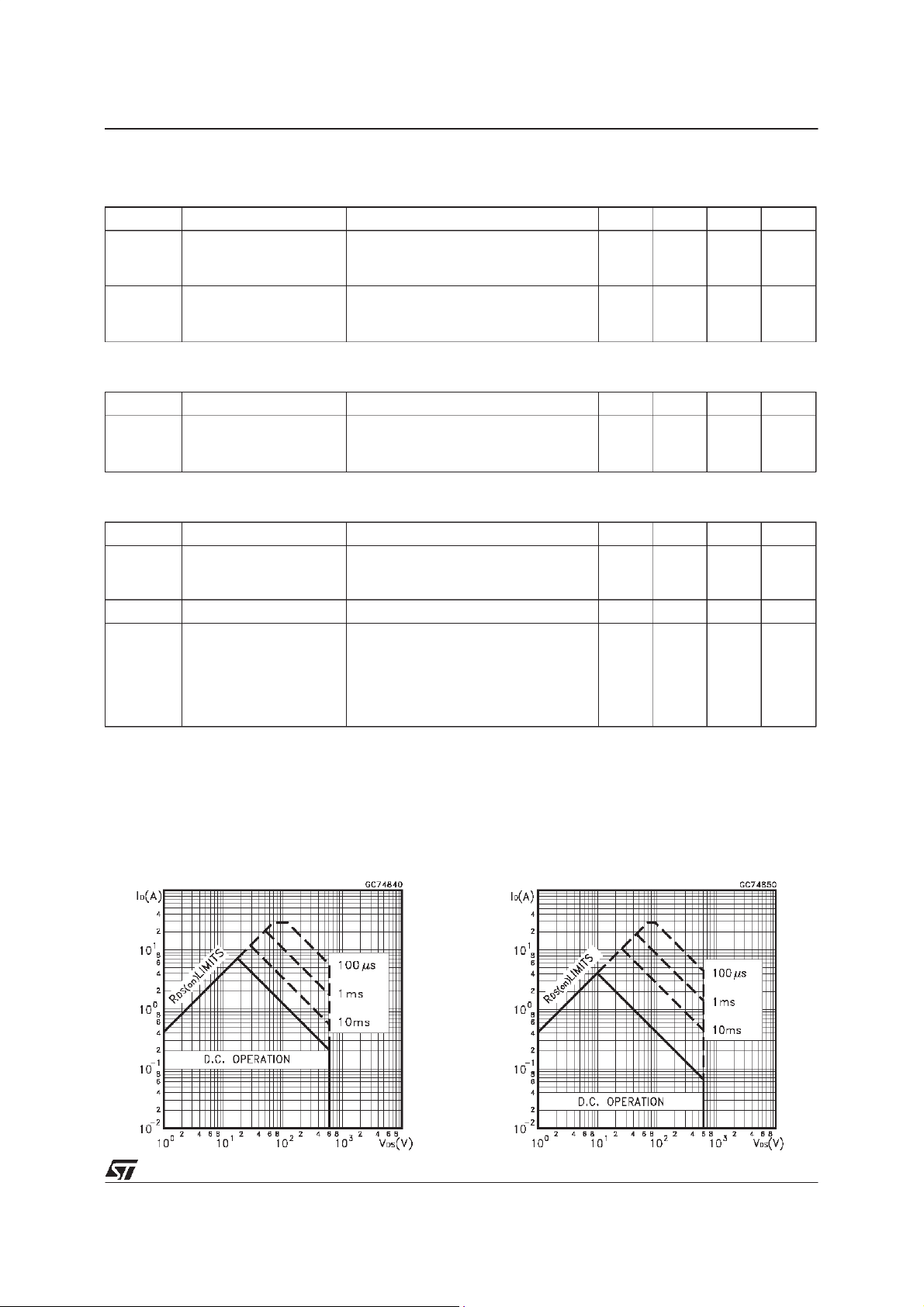
SafeOperating Area forTO-220 Safe OperatingArea for TO-220FP
3/9
 Loading...