

SGS-THOMSON STP6NA80, STP6NA80FI Technical data
现货库存、技术资料、百科信息、热点资讯,精彩尽在鼎好!
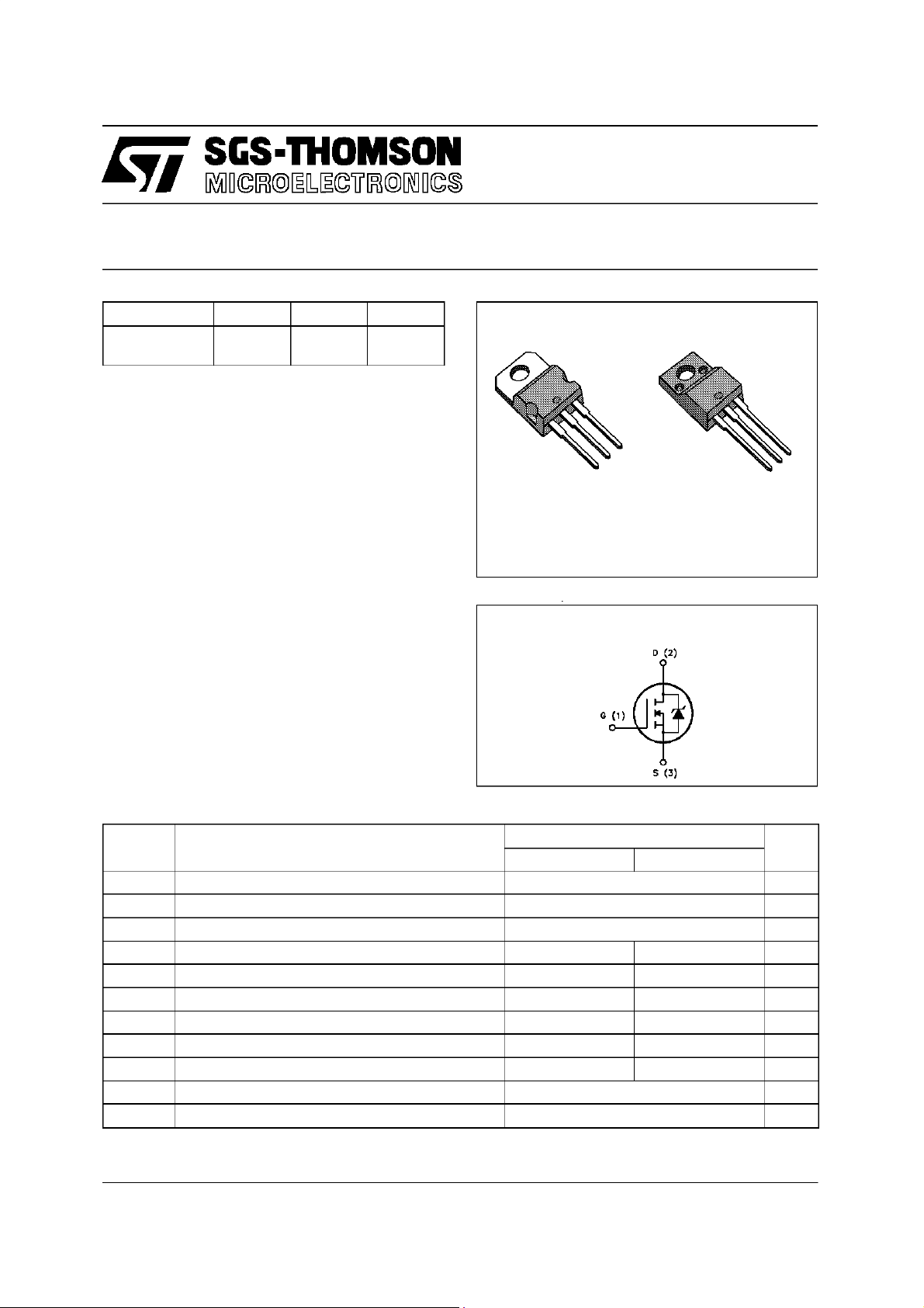
N - CHANNEL ENHANCEMENT MODE
FAST POWER MOS TRANSISTOR
STP6NA80
STP6NA80FI
TYPE V
STP 6NA80
STP 6NA80FI
■ TYPICAL R
■ ± 30V GATE TO SOURCE VOLTAGE RATING
■ 100% AVALANCHE TESTED
■ REPETITIVE AVALANCHE DATA AT 100
■ LOW INTRINSIC CAPACITANCES
■ GATE GHARGE MINIMIZED
■ REDUCED THRESHOLD VOLTAGE SPREAD
DS(on)
DSS
800 V
800 V
= 1.68 Ω
R
DS(on)
<1.9Ω
<1.9Ω
I
D
5.7 A
3.4 A
o
C
DESCRIPTION
This series of POWER MOSFETS represents the
most advanced high voltage technology. The
optimized cell layout coupled with a new
proprietary edge termination concur to give the
device low R
and gate charge, unequalled
DS(on)
ruggedness and superior switching performance.
APPLICATIONS
■ HIGH CURRENT, HIGH SPEED SWITCHING
■ SWITCH MODE POWERSUPPLIES (SMPS)
■ DC-AC CONVERTERS FOR WELDING
EQUIPMENT AND UNINTERRUPTIBLE
POWER SUPPLIES AND MOTOR DRIVE
3
2
1
TO-220 ISOWATT220
INTERNAL SCHEMATIC DIAGRAM
3
2
1
ABSOLUTE MAXIMUM RATINGS
Symb o l Paramet er Val u e Unit
ST P6NA80 ST P6NA80FI
V
V
V
I
DM
P
V
T
(•) Pulsewidth limited bysafe operating area
November 1996
Drain - s ource Voltage (VGS=0) 800 V
DS
Drain - gat e Voltage (RGS=20kΩ)800V
DGR
Gate-source Voltage ± 30 V
GS
Drain Current (continuous) at Tc=25oC5.73.4A
I
D
Drain Current (continuous) at Tc=100oC3.6 2.1A
I
D
(•) Drain Current (pulsed) 23 23 A
Total Di ssipation at Tc=25oC 125 45 W
tot
Derating F actor 1 0.36 W/
Ins ulation Withs t and Voltage (DC) 2000 V
ISO
St or a ge Tem perature -65 to 150
stg
Max. Operating Junction Temperature 150
T
j
o
o
o
C
C
C
1/10
STP6NA80/FI
THERMAL DATA
TO-220 ISOW ATT 220
R
thj-case
R
thj-amb
R
thc-sink
T
AVALANCHE CHARACTERISTICS
Symbol Parameter Max Value Uni t
I
AR
E
E
I
AR
Thermal Resistance J unction- c ase Max 1 2.78
Thermal Resistance Junc tion-am bie nt Max
Thermal Resistance Cas e-sink Typ
Maximum Lead T emperature For Soldering Purpose
l
Avalanc h e Cu rr ent , Repet itive or Not-R ep et itive
(pulse width limited by Tjmax, δ <1%)
Single Pul se Avalanche Ener gy
AS
(starti ng T
Repetitive Avalanc he Energ y
AR
=25oC, ID=IAR,VDD=50V)
j
(pulse width limited by Tjmax, δ <1%)
Avalanc h e Cu rr ent , Repet itive or Not-R ep et itive
(Tc= 100oC, pulse width limited by Tjmax, δ <1%)
62.5
0.5
300
5.7 A
165 mJ
6.5 mJ
3.6 A
o
C/W
o
C/W
o
C/W
o
C
ELECTRICAL CHARACTERISTICS (T
=25oC unless otherwise specified)
case
OFF
Symbol Parameter Test Conditions Min. Typ. Max. Unit
V
(BR)DSS
Drain - s ource
ID=250µAVGS= 0 800 V
Break d own Volta ge
I
DSS
I
GSS
Zer o Gate Volt age
Drain Current (VGS=0)
Gat e- body Leak age
Current (V
DS
=0)
VDS=MaxRating
VDS= Max Rating x 0 .8 Tc=125oC
= ± 30 V ± 100 nA
V
GS
25
250
ON (∗)
Symbol Parameter Test Conditions Min. Typ. Max. Unit
V
GS(th)
R
DS(on)
Gate Threshold Voltage VDS=VGSID=250µA 2.25 3 3.75 V
St at ic Drain-s our ce O n
VGS=10V ID=3A 1.68 1.9 Ω
Resistance
I
D(on)
On State Drain Current VDS>I
D(on)xRDS(on)max
6A
VGS=10V
DYNAMIC
Symbol Parameter Test Conditions Min. Typ. Max. Unit
(∗)Forward
g
fs
Tr ansconductance
C
C
C
Input Capacitance
iss
Out put Capacitance
oss
Reverse Transfer
rss
Capacitance
VDS>I
D(on)xRDS(on)maxID
=3A 4 6.1 S
VDS=25V f=1MHz VGS= 0 1330
160
40
1750
210
55
µA
µA
pF
pF
pF
2/10
STP6NA80/FI
ELECTRICAL CHARACTERISTICS (continued)
SWITCHING ON
Symbol Parameter Test Conditions Min. Typ. Max. Unit
t
d(on)
(di/dt)
Q
Q
Q
Turn-on T im e
t
Rise Time
r
Turn-on C urrent S lope VDD=640V ID=6A
on
Total Gate Charge
g
Gat e- Source Charge
gs
Gate-Drain Charge
gd
SWITCHING OFF
Symbol Parameter Test Conditions Min. Typ. Max. Unit
t
r(Voff)
t
Off -voltage R ise Time
t
Fall Time
f
Cross-over Time
c
SOURCE DRAIN DIODE
VDD=400V ID=3A
RG=47 Ω VGS=10V
35
95
(see test circuit, figure 3)
170 A/µs
RG=47 Ω VGS=10V
(see test circuit, figure 5)
VDD= 640 V ID=6A VGS=10V 58
8
27
VDD=640V ID=6A
RG=47 Ω VGS=10V
(see test circuit, figure 5)
90
25
125
45
125
78 nC
120
35
165
ns
ns
nC
nC
ns
ns
ns
Symbol Parameter Test Conditions Min. Typ. Max. Unit
I
I
SDM
SD
Source-drain Current
(•)
Source-drain Current
5.7
23
(pulsed)
V
(∗) Forward On Voltage ISD=6A VGS=0 1.6 V
SD
t
Reverse Recovery
rr
Time
Q
Reverse Recovery
rr
ISD=6A di/dt=100A/µs
VDD= 100 V Tj=150oC
(see test circuit, figure 5)
850
15
Charge
I
RRM
Reverse Recovery
35
Current
(∗) Pulsed:Pulse duration = 300 µs, dutycycle 1.5 %
(•) Pulse widthlimited by safeoperating area
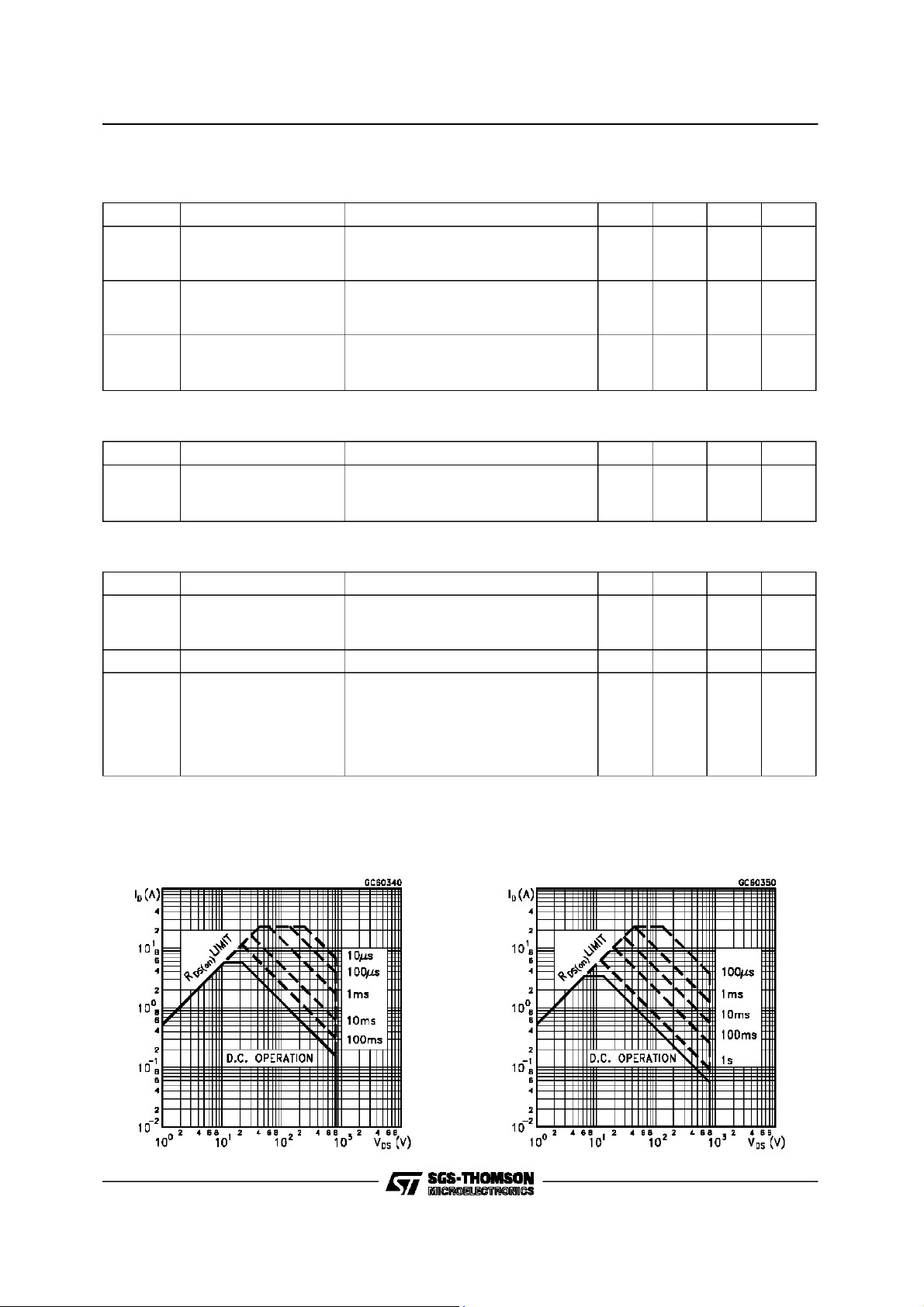
Safe Operating Areas for TO-220 Safe Operating Areas for ISOWATT220
A
A
ns
µC
A
3/10
 Loading...