

查询ST93CS66供应商
4K (256 x 16) SERIAL MICROWIRE EEPROM
1 MILLIONERASE/WRITE CYCLES, with
40 YEARS DATARETENTION
SELF-TIMED PROGRAMMINGCYCLE with
AUTO-ERASE
READY/BUSYSIGNALDURING
PROGRAMMING
SINGLESUPPLYVOLTAGE
– 3V to 5.5V for the ST93CS66
– 2.5V to 5.5V for the ST93CS67
USER DEFINEDWRITE PROTECTED AREA
PAGEWRITE MODE (4 WORDS)
SEQUENTIALREAD OPERATION
5ms TYPICALPROGRAMMINGTIME
ST93CS66and ST93CS67 are replaced by
the M93S66
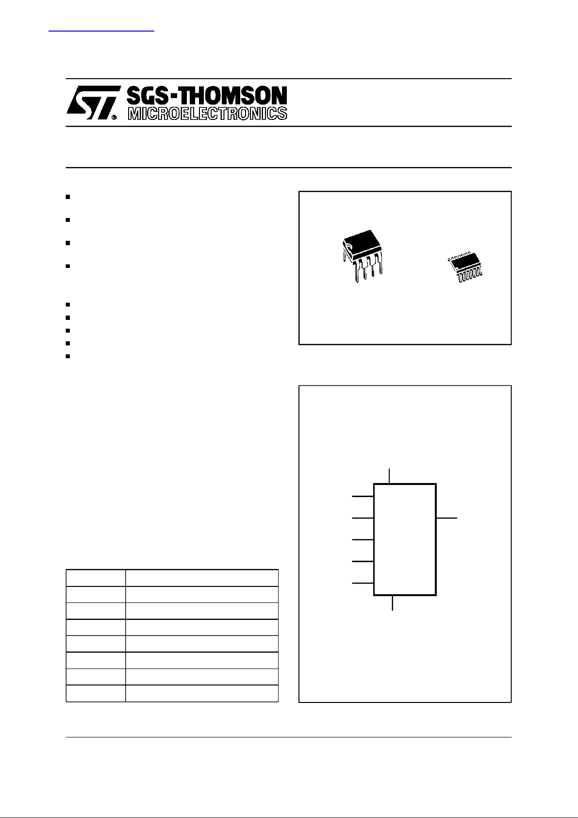
8
1
PSDIP8 (B)
0.25mm Frame
Figure 1. Logic Diagram
ST93CS66
ST93CS67
NOT FOR NEW DESIGN
14
1
SO14 (ML)
150mil Width
DESCRIPTION
The ST93CS66 and ST93CS67 are 4K bit ElectricallyErasable ProgrammableMemory(EEPROM)
fabricatedwithSGS-THOMSON’sHighEndurance
SinglePolysiliconCMOStechnology.The memory
is accessed through a serial inputD and outputQ.
The 4K bit memory is organized as 256 x 16 bit
words.Thememory is accessedby aset of instructionswhich include Read, Write, Page Write, Write
Allandinstructionsused to set thememoryprotection. A Read instruction loads the address of the
first word to be read into an internal address
pointer.
Table 1. Signal Names
S Chip Select Input
D Serial Data Input
Q Serial Data Output
C Serial Clock
PRE Protect Enable
W Write Enable
V
CC
V
SS
Supply Voltage
Ground
V
CC
D
CQ
S
PRE
W
ST93CS66
ST93CS67
V
SS
AI00906B
June 1997 1/16
This isinformation on a productstill in productionbutnot recommendedfor new designs.
ST93CS66,ST93CS67
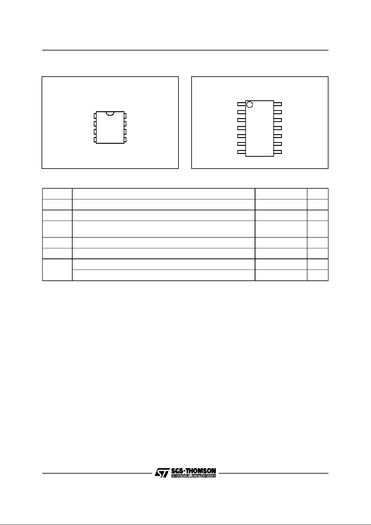
Figure 2A. DIP Pin Connections
Figure2B. SO PinConnections
ST93CS66
ST93CS67
ST93CS66
ST93CS67
SV
1
2
D
3
Q
4
Table 2. Absolute Maximum Ratings
Symbol Parameter Value Unit
T
T
STG
T
LEAD
V
V
CC
V
ESD
Notes: 1. Exceptfor the rating ”Operating Temperature Range”, stresses above those listed in the Table ”Absolute Maximum Ratings”
Ambient Operating Temperature –40 to85 °C
A
Storage Temperature –65 to150 °C
Lead Temperature,Soldering (SO14 package)
Input or Output Voltages(Q = VOHor Hi-Z) –0.3 to VCC+0.5 V
IO
Supply Voltage –0.3 to 6.5 V
Electrostatic Discharge Voltage (Human Body model)
Electrostatic Discharge Voltage (Machine model)
may cause permanent damage to the device. These are stressratings only and operation of thedevice at these or any other
conditions abovethose indicated in the Operating sections of this specification is not implied. Exposure toAbsolute Maximum
Rating conditions for extended periods may affect device reliability.Refer also to the SGS-THOMSON SURE Program and other
relevant quality documents.
2. MIL-STD-883C, 3015.7(100pF, 1500 Ω).
3. EIAJ IC-121 (Condition C) (200pF, 0 Ω).
8
7
6
5
AI00907B
PREC
W
V
CC
SS
Warning: NC = Not Connected.
(1)
(PSDIP8 package)
(2)
(3)
NC
NC
40 sec
10 sec
1
14
NC
2
S
3
C
4
DW
5
QV
6
7
AI00908C
V
13
12
11
CC
PRE
NC
10
9
SS
8NCNC
215
260
2000 V
500 V
°C
DESCRIPTION (cont’d)
The data is then clocked out serially. The address
pointer is automaticallyincremented after the data
is output and, if the Chip Select input (S) is held
High, the ST93CS66/67 can output a sequential
streamof data words. In thisway,thememory can
be read as a data stream of 16 to 4096 bits, or
continuouslyas the addresscounterautomatically
rolls over to 00 when the highest address is
reached.
Within the time required by a programming cycle
(t
), up to 4 wordsmay be written with the help of
W
the Page Write instruction;thewhole memorymay
alsobe erased,or set to a predetermined pattern,
by using the WriteAll instruction.
Within the memory, an user defined area may be
protected against further Write instructions. The
2/16
size of this area is defined by the content of a
Protect Register, located outside of the memory
array. As a final protection step, data may be permanently protected by programming a One Time
Programing bit (OTP bit) which locks the Protect
Registercontent.
Programming is internally self-timed (the external
clocksignal on Cinput may be disconnectedorleft
running after the start of a Write cycle) and does
notrequirean erasecyclepriorto the Writeinstruction.TheWriteinstructionwrites 16bits at onetime
intoone of the 256 words, the PageWrite instruction writes up to 4 words of 16 bits to sequential
locations, assuming in both cases that all addressesareoutsidetheWrite Protectedarea. After
the start of the programming cycle, a Ready/Busy
signalis availableon the Data output(Q) when the
ChipSelect (S)input pin is driven High.
ST93CS66, ST93CS67
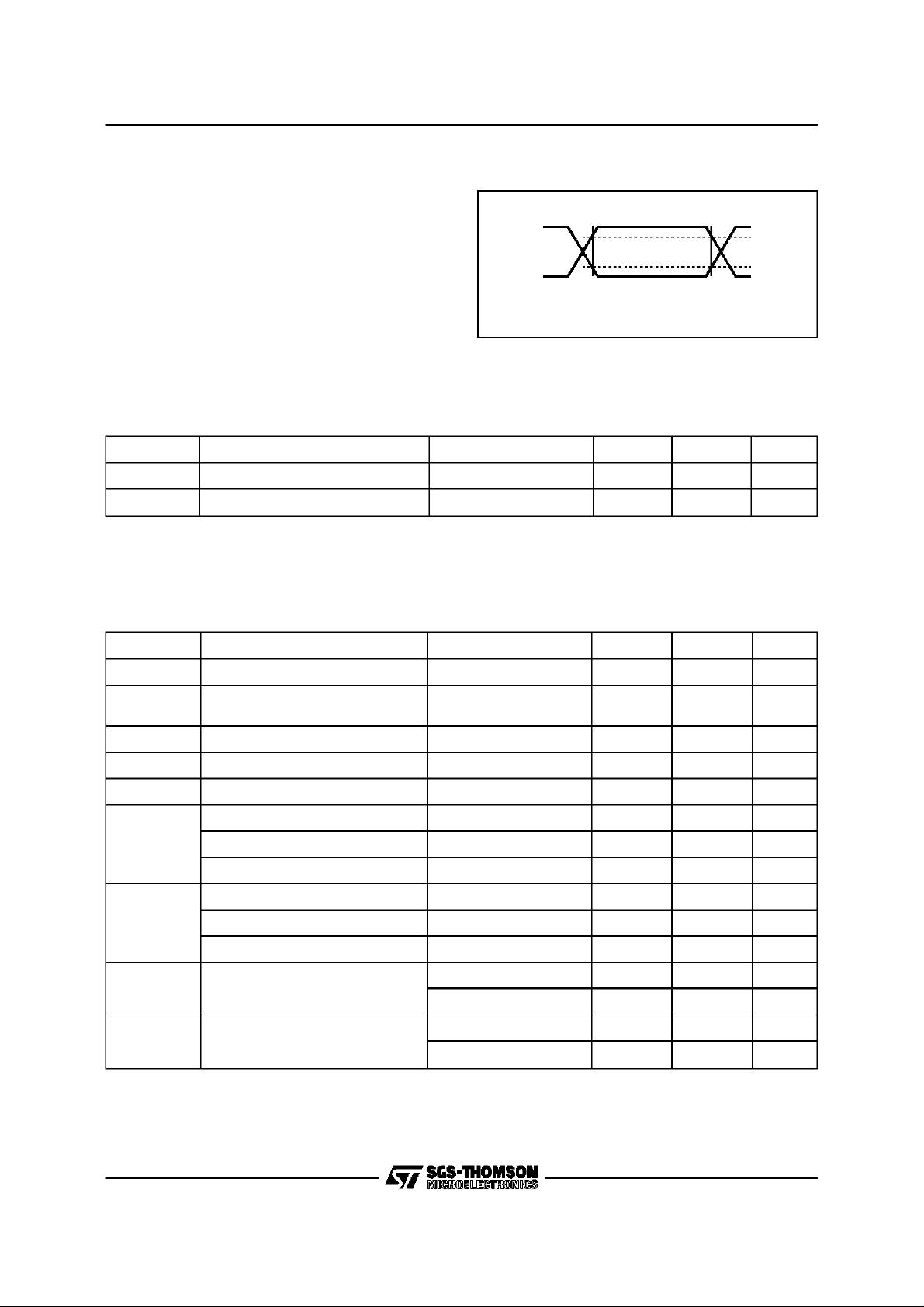
AC MEASUREMENT CONDITIONS
Figure 3. ACTesting Input Output Waveforms
Input Rise and Fall Times ≤ 20ns
0.8V
0.2V
CC
CC
0.7V
0.3V
AI00825
0.3V
CC
CC
to 0.8V
to 0.7V
CC
CC
Input Pulse Voltages 0.2V
Input and Output Timing
Reference Voltages
Note that Output Hi-Z is defined as the point where data
is no longer driven.
Table 3. Capacitance
(1)
(TA=25°C, f =1 MHz)
Symbol Parameter Test Condition Min Max Unit
C
IN
C
OUT
Note: 1. Sampled only, not 100% tested.
Input Capacitance VIN=0V 5 pF
Output Capacitance V
=0V 5 pF
OUT
Table 4. DC Characteristics(TA= 0 to 70°C or –40 to 85°C; VCC=3V to 5.5V for ST93CS66 and
= 2.5Vto 5.5V for ST93CS67)
V
CC
Symbol Parameter TestCondition Min Max Unit
I
I
I
CC1
V
V
V
V
I
LI
LO
CC
IL
IH
OL
OH
Input Leakage Current 0V ≤ VIN≤ V
Output Leakage Current
0V ≤ V
≤ VCC,
OUT
Q inHi-Z
CC
±2.5 µA
±2.5 µA
Supply Current (TTL Inputs) S = VIH, f = 1 MHz 3 mA
Supply Current (CMOS Inputs) S = V
Supply Current (Standby) S = VSS,C=V
, f = 1 MHz 2 mA
IH
SS
50 µA
Input Low Voltage (ST93CS66,67) 4.5V ≤ VCC≤ 5.5V –0.1 0.8 V
Input Low Voltage (ST93CS66) 3V ≤ V
Input Low Voltage (ST93CS67) 2.5V ≤ V
≤ 5.5V –0.1 0.2 V
CC
≤ 5.5V –0.1 0.2 V
CC
CC
CC
Input High Voltage (ST93CS66,67) 4.5V ≤ VCC≤ 5.5V 2 VCC+1 V
Input High Voltage (ST93CS66) 3V ≤ V
Input High Voltage (ST93CS67) 2.5V ≤ V
Output Low Voltage
Output High Voltage
I
≤ 5.5V 0.8 V
CC
≤ 5.5V 0.8 V
CC
I
= 2.1mA 0.4 V
OL
I
=10µA 0.2 V
OL
= –400µA 2.4 V
OH
I
= –10µAV
OH
CC
CC
–0.2 V
CC
VCC+1 V
VCC+1 V
CC
CC
V
V
3/16
ST93CS66,ST93CS67
Table 5. ACCharacteristics (TA=0 to70° or,–40 to 85°C; VCC= 3V to 5.5V for ST93CS66 and
V
= 2.5Vto 5.5V for ST93CS67)
CC
Symbol Alt Parameter Test Condition Min Max Unit
t
PRVCH
t
WVCH
t
SHCH
t
DVCH
t
CHDX
t
CHQL
t
CHQV
t
CLPRX
t
SLWX
t
CLSL
t
SLSH
t
SHQV
t
SLQZ
t
CHCL
t
CLCH
t
W
f
C
Notes: 1. Chip Select must be brought low for a minimum of 250 ns (t
2. The Clock frequency specification calls for a minimum clockperiod of 1 µs, therefore the sum of the timings t
t
PRES
t
PES
t
CSS
t
DIS
t
DIH
t
PD0
t
PD1
t
PREH
t
PEH
t
CSH
t
CS
t
SV
t
DF
t
SKH
t
SKL
t
WP
f
SK
must be greater or equal to 1 µs. For example, ift
Protect Enable Valid to Clock High 50 ns
Write Enable Validto Clock High 50 ns
Chip Select High to Clock High 50 ns
Input Valid to Clock High 100 ns
Clock High to Input Transition 100 ns
Clock High to Output Low 500 ns
Clock High to Output Valid 500 ns
Clock Low to Protect Enable Transition 0 ns
Chip Select Low to Write Enable Transition 250 ns
Clock Low to Chip Select Transition 0 ns
Chip Select Low to Chip Select High Note 1 250 ns
Chip Select High to Output Valid 500 ns
Chip Select Low to Output Hi-Z 300 ns
Clock High to Clock Low Note 2 250 ns
Clock Low to Clock High Note 2 250 ns
Erase/Write Cycle time 10 ms
Clock Frequency 0 1 MHz
) betweenconsecutive instructioncycles.
is 250 ns, then t
CHCL
SLSH
must be at least 750ns.
CLCH
CHCL+tCLCH
Figure4. Synchronous Timing,Start and Op-Code Input
PRE
tPRVCH
W
C
tSHCH tCLCH
S
D
START
4/16
OP CODE OP CODESTART
OP CODE INPUT
tCHCLtWVCH
tCHDXtDVCH
AI00887
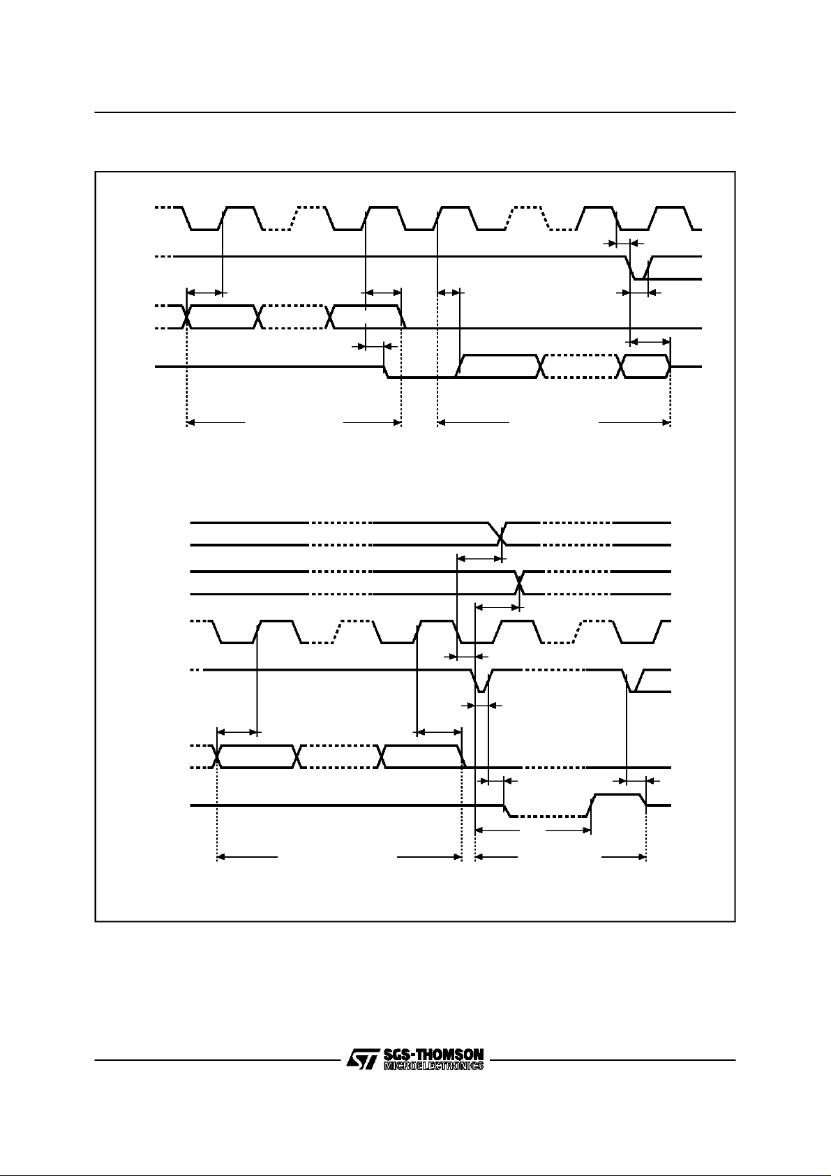
Figure5. Synchronous Timing,Read or Write
C
S
ST93CS66, ST93CS67
tCLSL
D
Q
PRE
W
C
S
Hi-Z
tDVCH
An
ADDRESS INPUT
tCHQL
A0
tCHQVtCHDX
tSLQZ
Q15/Q7 Q0
DATA OUTPUT
tCLPRX
tSLWX
tCLSL
tSLSH
tSLSH
AI00820C
tDVCH
D
Q
An A0/D0
Hi-Z
tCHDX
tSHQV
BUSY
tW
WRITE CYCLEADDRESS/DATA INPUT
tSLQZ
READY
AI00888B
5/16

ST93CS66,ST93CS67
POWER-ON DATAPROTECTION
In order to preventdatacorruptionand inadvertent
write operations during power up, a Power On
Reset(POR)circuit resetsall internalprogramming
circuitry and sets the device in the Write Disable
mode. When V
reaches its functionalvalue, the
CC
deviceisproperlyreset (inthe Write Disablemode)
and is ready to decode and execute an incoming
instruction. A stable V
must be applied before
CC
anylogic signal.
appliedon the ChipSelect(S) input(assumingthat
the Clock C is low). The data input D is then
sampled upon the following rising edges of the
clock C until a ’1’ is sampled and decoded by the
ST93CS66/67as a Start bit.
TheST93CS66/67is fabricated in CMOS technologyandisthereforeableto runfromzeroHz (static
inputsignals)up to the maximumratings(specified
in Table 5).
Read
The Read instruction (READ) outputs serial data
INSTRUCTIONS
The ST93CS66/67 has eleven instructions, as
shownin Table 6. Each instructionis composedof
a 2 bit op-code and an 8bit address. Each instruc-
on the Data Output (Q). Whena READ instruction
is received, the instruction and address are decodedandthedata fromthememoryistransferred
intoanoutputshiftregister.Adummy’0’bitisoutput
firstfollowedby the 16 bit word with the MSB first.
tion is preceded by the rising edge of the signal
Table 6. InstructionSet
(1)
PRE
pinOpCode
Address
Instruction Description
READ Read Data from Memory X ’0’ 10 A7-A0 Q15-Q0
WRITE Write Data to Memory ’1’ ’0’ 01 A7-A0 D15-D0
W
pin
(1)
Data
Additional
Information
Write is executed if
the address is not
inside the
Protected area
PAWRITE Page Write to Memory ’1’ ’0’ 11 A7-A0 D15-D0
WRALL WriteAll Memory ’1’ ’0’ 00 01XX XXXX D15-D0
WEN Write Enable ’1’ ’0’ 00 11XX XXXX
WDS Write Disable X ’0’ 00 00XX XXXX
PRREAD Protect RegisterRead X ’1’ 10 XXXX XXXX Q8-Q0
PRWRITE Protect Register Write ’1’ ’1’ 01 A7-A0
PRCLEAR Protect RegisterClear ’1’ ’1’ 11 1111 1111
PREN Protect RegisterEnable ’1’ ’1’ 00 11XX XXXX
PRDS Protect RegisterDisable ’1’ ’1’ 00 0000 0000
Note: 1. X = don’t care bit.
Write is executed if
all the addresses
are not inside the
Protected area
Write alldata ifthe
Protect Register is
cleared
Data Output =
Protect Register
content + Protect
Flag bit
Data above
specified address
A7-A0 are
protected
Protect Flag is also
cleared (cleared
Flag = 1)
OTP bit is set
permanently
6/16

ST93CS66, ST93CS67
Output data changes are triggered by the Low to
High transitionof theClock(C). The ST93CS66/67
will automatically increment the address and will
clockout the next wordas long as the Chip Select
input (S)is held High.Inthiscasethedummy ’0’bit
is NOT output between words and a continuous
streamof data can be read.
Write Enable and Write Disable
The WriteEnableinstruction(WEN) authorizesthe
following Write instructions to be executed, the
Write Disable instruction (WDS) disables the execution of the following Erase/Write instructions.
When power is first applied, the ST93CS66/67
enters the Disable mode. When the Write Enable
instruction (WEN) is executed, Write instructions
remain enabled until a Write Disable instruction
(WDS) is executed or if the Power-on reset circuit
becomes active due to a reduced V
. Toprotect
CC
the memory contentsfrom accidentalcorruption,it
is advisable to issue the WDS instruction after
everywrite cycle.
The READ instruction is not affected by the WEN
or WDSinstructions.
Write
The Write instruction (WRITE) is followed by the
address and the word to be written. The Write
Enable signal (W) must be held high during the
WRITEinstruction.DatainputD is sampledon the
Low to High transition of the clock. After the last
data bit has been sampled, Chip Select (S) must
be brought Low before the nextrising edge of the
clock(C), inorder to startthe self-timedprogrammingcycle,providingthattheaddressis NOTin the
protected area. If the ST93CS66/67 is still performingtheprogrammingcycle,theBusysignal (Q
= 0) will be returnedif the Chip Select input (S) is
drivenhigh, and the ST93CS66/67will ignore any
dataon the bus.Whenthewritecycle iscompleted,
the Ready signal(Q = 1) willindicate (if S is driven
high) that the ST93CS66/67is ready to receive a
new instruction.
Page Write
APage Write instruction(PAWRITE) containsthe
firstaddress to be writtenfollowed by up to 4 data
words. The Write Enable signal (W) must be held
HighduringtheWriteinstruction.Inputaddressand
data are read on the Low to High transition of the
clock. After the receipt of each data word, bits
A1-A0 of the internal address register are incremented, the high order bits A7-A2 remaining unchanged. Users must take care by software to
ensurethat the last wordaddresshas the samesix
upper order address bits as the initial address
transmittedto avoid address roll-over.
After the LSB of the last data word, Chip Select(S)
must be broughtLowbeforethenextrisingedge of
the Clock (C). The falling edge of Chip Select (S)
initiates the internal, self-timed write cycle. The
Page Write operation will not be performed if any
of the 4 words is addressing the protectedarea.If
the ST93CS66/67 is still performing the programming cycle, the Busysignal (Q = 0)will be returned
if the Chip Select input (S) is driven high, and the
ST93CS66/67 will ignore any data on the bus.
When the write cycle is completed, the Ready
signal (Q = 1) will indicate (if S is drivenhigh) that
the ST93CS66/67isreadytoreceivea newinstruction.
Write All
The WriteAll instruction(WRALL) isvalid onlyafter
the ProtectRegisterhas beenclearedbyexecuting
a PRCLEAR (Protect Register Clear) instruction.
The WriteAll instructionsimultaneouslywrites the
whole memory with the same data word included
in the instruction. The Write Enable signal (W)
must be held High before and during the Write
instruction.Input addressand dataare read on the
Low to High transition of the clock. If the
ST93CS66/67is still performing the programming
cycle, the Busysignal (Q = 0) will be returnedifthe
Chip Select input (S) is driven high, and the
ST93CS66/67 will ignore any data on the bus.
When the write cycle is completed, the Ready
signal (Q = 1) will indicate (if S is drivenhigh) that
the ST93CS66/67isreadytoreceivea newinstruction.
MEMORYWRITEPROTECTIONANDPROTECT
REGISTER
The ST93CS66/67offers a Protect Register containing the bottom address of the memory area
which has to be protected against write instructions. In addition to this Protect Register, two flag
bitsareusedtoindicatetheProtectRegisterstatus:
the Protect Flag enabling/disablingthe protection
of theProtectRegister andtheOTPbit which,when
set, disables access to the Protect Register and
thus preventsany furthermodificationsof this Protect Register value. The content of the Protect
Register is defined when using the PRWRITE instruction,it may be read when using thePRREAD
instruction. A specific instruction PREN (Protect
Register Enable) allows the user to execute the
protect instructions PRCLEAR, PRWRITE and
PRDS; this PREN instruction beingused together
with the signals applied on the input pins PRE
(Protect Register Enable pin) and W (Write Enable).
7/16

ST93CS66,ST93CS67
Figure6. READ, WRITE, WEN, WDS Sequences
PREREAD
S
WRITE
D
Q
PRE
W
S
D
Q
110An A0
ADDR
OP
CODE
1 0 An A0
AD D R
OP
CODE
Qn Q0
DATA OUT
Dn D01
DATA IN
CHECK
STATUS
BUSY READY
8/16
WRITE
ENABLE
PRE
W
S
1 0 Xn X0D
OP
CODE
WRITE
DISABLE
101
PRE
S
000
1 0 Xn X0D
OP
CODE
AI00889D

Figure7. PAWRITE, WRALL Sequences
ST93CS66, ST93CS67
PAGE
WRITE
WRITE
ALL
PRE
W
S
D
Q
PRE
W
1 1 An A0
ADDR
OP
CODE
CHECK
STATUS
Dn D01
DATA IN
BUSY READY
S
CHECK
STATUS
D
Q
1 0 Xn X0
01
ADDR
OP
CODE
Dn D00
DATA IN
BUSY READY
AI00890C
9/16

ST93CS66,ST93CS67
MEMORY WRITE PROTECTION(cont’d)
Accessingthe Protect Register is done by executing the followingsequence:
– WEN: executethe Write Enableinstruction,
– PREN: executethe PREN instruction,
– PRWRITE, PRCLEAR or PRDS:the protection
then maybe defined, in termsof sizeof the
protected area (PRWRITE, PRCLEAR) and
may be set permanently(PRDS instruction).
ProtectRegisterRead
The Protect Register Read instruction (PRREAD)
outputs on the Data Output Q the content of the
Protect Register, followed by the Protect Flag bit.
The Protect Register Enable pin (PRE) must be
drivenHighbeforeandduringtheinstruction.Asin
the Read instructiona dummy ’0’ bit is output first.
Sinceit is not possible to distinguish if the Protect
Registeris cleared(all 1’s) or ifit is written with all
1’s, user must check the Protect Flag status (and
not the Protect Register content) to ascertainthe
settingof the memory protection.
ProtectRegisterEnable
The Protect Register Enableinstruction(PREN) is
used to authorize the use of further PRCLEAR,
PRWRITE and PRDS instructions. The PREN
insruction does not modify the Protect Flag bit
value.
Note: A Write Enable (WEN) instruction must be
executed before the Protect Enable instruction.
Both the Protect Enable (PRE) and Write Enable
(W)inputpinsmustbeheld Highduringthe instructionexecution.
ProtectRegisterClear
TheProtectRegisterClear instruction (PRCLEAR)
clearstheaddressstored in theProtectRegister to
all 1’s, and thus enables the execution of WRITE
and WRALL instructions. The Protect Register
Clear executionclears the ProtectFlag to ’1’. Both
the Protect Enable (PRE) and Write Enable (W)
input pins must be driven High during the instructionexecution.
Note: A PREN instruction must immediately precede the PRCLEARinstruction.
ProtectRegisterWrite
The Protect RegisterWriteinstruction(PRWRITE)
is used to write into the Protect Register the address of the first word to be protected. After the
PRWRITE instructionexecution, all memory locationsequalto andabovethespecifiedaddress,are
protectedfrom writing.TheProtect Flag bit isset to
’0’, it can be read with Protect Register Read
instruction. Both the Protect Enable (PRE) and
Write Enable (W) input pins must be driven High
duringthe instructionexecution.
Note: A PREN instruction must immediately precede the PRWRITEinstruction,but it isnot necessary to execute first a PRCLEAR.
ProtectRegister Disable
The Protect Register Disable instruction sets the
OneTime Programmable bit (OTPbit).TheProtect
RegisterDisableinstruction(PRDS) isaONETIME
ONLYinstruction which latchesthe Protect Register content, this content is therefore unalterable in
thefuture.BoththeProtectEnable(PRE)andWrite
Enable(W) input pins must be driven High during
the instruction execution. The OTP bit cannot be
directly read, it can be checked by reading the
content of the Protect Register (PRREAD instruction),then by writing this same value into the Protect Register (PRWRITE instruction): when the
OTP bit is set, the Ready/Busystatus cannot appear on the Data output (Q); when the OTP bit is
not set, the Busystatus appear on the Data output
(Q).
APREN instruction must immediatelyprecede the
PRDSinstruction.
READY/BUSY Status
When the ST93CS66/67 is performing the write
cycle, the Busy signal (Q = 0) is returned if S is
drivenhigh, and the ST93CS66/67will ignore any
dataon thebus.Whenthewritecycleiscompleted,
the Ready signal (Q =1) will indicate, if S is driven
high, that the ST93CS66/67is ready to receive a
newinstruction.Oncethe ST93CS66/67is Ready,
the Data OutputQ is set to ’1’ until a newStart bit
isdecoded or theChip Select is brought Low.
COMMONI/O OPERATION
TheDataOutput(Q)andDataInput(D) signalscan
be connected together, through a current limiting
resistor, to form a common, one wire data bus.
Some precautions must be taken when operating
the memorywiththis connection,mostlyto prevent
a shortcircuit between thelastenteredaddressbit
(A0) and the first data bit output by Q.The reader
should refer to the SGS-THOMSON application
note”MICROWIREEEPROMCommon I/OOperation”.
10/16

Figure8. PRREAD, PRWRITE, PREN Sequences
ST93CS66, ST93CS67
Protect
Register
READ
Protect
Register
WRITE
PRE
S
D
Q
PRE
W
S
110Xn X0
ADDR
OP
CODE
1 0 An A0D
1
An A0 F
DATA
OUT
CHECK
STATUS
F = Protect Flag
Protect
Register
ENABLE
Q
PRE
W
S
OP
CODE
1 0 Xn X0D
OP
CODE
ADDR
101
BUSY READY
AI00891D
11/16

ST93CS66,ST93CS67
Figure 9. PRCLEAR, PRDS Sequences
Protect
Register
CLEAR
Protect
Register
DISABLE
PRE
W
S
Q
PRE
W
S
1
11D
OP
CODE
10D
0
ADDR
CHECK
STATUS
111
BUSY READY
CHECK
STATUS
000
12/16
Q
OP
CODE
ADDR
BUSY READY
AI00892C

ORDERING INFORMATION SCHEME
Example: ST93CS66 M 1 013TR
ST93CS66, ST93CS67
Operating Voltage
66 3V to 5.5V
67 2.5V to 5.5V
Note: 1. Temperature range on request only.
Package
B PSDIP8
0.25mm
Frame
ML SO14
150mil Width
Temp. Range
1 0 to 70 °C
6 –40 to 85 °C
(1)
3
–40 to 125 °C
Option
013TR Tape & Reel
Packing
Devicesare shippedfrom the factory with the memory content set at all ”1’s” (FFFFh).
For a list of availableoptions (OperatingVoltage,Package,etc...) orfor further information on any aspect
of thisdevice, please contact theSGS-THOMSON Sales Office nearestto you.
13/16

ST93CS66,ST93CS67
PSDIP8 - 8 pin PlasticSkinny DIP, 0.25mm lead frame
Symb
Typ Min Max Typ Min Max
A 3.90 5.90 0.154 0.232
A1 0.49 – 0.019 –
A2 3.30 5.30 0.130 0.209
B 0.36 0.56 0.014 0.022
B1 1.15 1.65 0.045 0.065
C 0.20 0.36 0.008 0.014
D 9.20 9.90 0.362 0.390
E 7.62 – – 0.300 – –
E1 6.00 6.70 0.236 0.264
e1 2.54 – – 0.100 – –
eA 7.80 – 0.307 –
eB 10.00 0.394
L 3.00 3.80 0.118 0.150
N8 8
CP 0.10 0.004
PSDIP8
mm inches
Drawing is not to scale
14/16
A2A1A
L
B
e1
B1
D
N
C
eA
eB
E1 E
1
PSDIP-a

ST93CS66, ST93CS67
SO14 - 14 lead Plastic Small Outline, 150mils body width
Symb
Typ Min Max Typ Min Max
A 1.35 1.75 0.053 0.069
A1 0.10 0.25 0.004 0.010
B 0.33 0.51 0.013 0.020
C 0.19 0.25 0.007 0.010
D 8.55 8.75 0.337 0.344
E 3.80 4.00 0.150 0.157
e 1.27 – – 0.050 – –
H 5.80 6.20 0.228 0.244
h 0.25 0.50 0.010 0.020
L 0.40 0.80 0.016 0.031
α 0° 8° 0° 8°
N14 14
CP 0.10 0.004
SO14
mm inches
Drawing is not to scale
B
SO-a
hx45°
A
C
e
CP
D
N
E
H
1
LA1 α
15/16

ST93CS66,ST93CS67
Information furnished is believed to be accurate and reliable.However, SGS-THOMSON Microelectronics assumes no responsibility for the
consequences of use of such information nor for any infringementof patents or other rights of third parties which may result from its use.No
license is granted by implication or otherwise under any patentor patent rights ofSGS-THOMSON Microelectronics. Specificationsmentioned
in this publication are subject to change without notice. This publication supersedes and replaces all information previously supplied.
SGS-THOMSON Microelectronics productsare notauthorized foruse ascritical components in life supportdevices or systemswithout express
written approval of SGS-THOMSONMicroelectronics.
1997 SGS-THOMSON Microelectronics - All Rights Reserved
MICROWIRE isa registered trademark of National SemiconductorCorp.
Australia - Brazil - Canada- China - France - Germany - Hong Kong - Italy - Japan - Korea- Malaysia - Malta - Morocco - The Netherlands -
Singapore- Spain - Sweden - Switzerland - Taiwan- Thailand - United Kingdom - U.S.A.
SGS-THOMSON Microelectronics GROUP OF COMPANIES
16/16
 Loading...